Bipolar Junction Transistors: 1 + 1 > 2
 2026-06-04
  electronics, semiconductor, notes
This is a summary note of the bipolar junction transistor part in the course “Ve311 Electronic Circuits,” introducing the basic working principles of a BJT and its circuit model.
Note: You may view the Chinese translation of the post here, but it is only for reference.
Bipolar Junction Transistors (BJT)
Structure
Imagine sandwiching a block of p-type material between two blocks of n-type materials. When the p-type block is wide, the whole structure is functionally equivalent to two independent PN junctions with their anodes connected. However, interesting coupling effects will occur between the two PN junctions when the p-type block becomes very narrow.
A bipolar junction transistor (BJT) takes the exact structure as this “sandwich”, consisting of three blocks of doped materials each acting as a terminal. Let’s put the p-type material in the middle first, which is known as an NPN BJT.
| Name | Position | Dope type | Dope level | Description |
|---|---|---|---|---|
| Emitter (E) | side | n | heavy | emit electrons |
| Base (B) | middle | p | mild | narrow region |
| Collector (C) | side | n | mild | receive electrons |
At equilibrium, the Fermi levels of the three regions match, resulting in a bump in the electron energy of the base region. Due to the size of the base region, the width of the “bump” is narrow, so there is a possibility of diffused electrons from the emitter region to cross the base region without recombining with holes and get swept into the collector region.
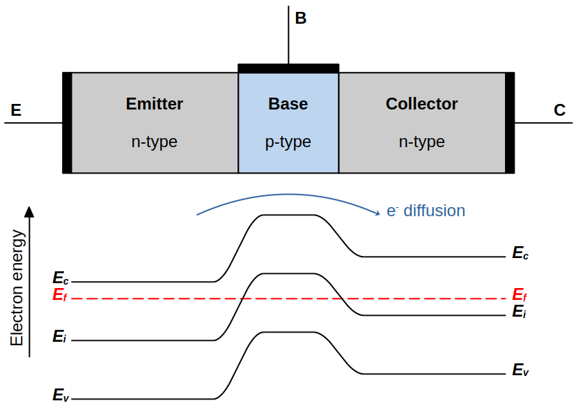
Visualization of the energy levels of a NPN BJT.
Operating Regions
Depending on the voltage biases on the two PN junctions (BE and BC), the BJT works in four operating regions, each with different characteristics:
| Operating region | BE bias | BC bias | Characteristics |
|---|---|---|---|
| Forward Active | forward | reverse | current amplifier |
| Saturation | forward | forward | closed switch |
| Cutoff | reverse | reverse | open switch |
| Reverse Active | reverse | forward | similar to forward active but not optimal |
Forward Active and Reverse Active
Consider forward active region first, where
- BE forward-biased (\(v_{BE} > 0.7\,\mathrm{V}\)): large amount of electrons injected into base region; and
- BC reverse-biased (\(v_C > v_B\)): large depletion zone with large electric field.
💡 In practice, a slight forward bias is also tolerated by the BC junction for the BJT to work in the forward active region, with the voltage \(v_{CE} \approx 0.3\,\mathrm{V}\) as the threshold (i.e. \(v_{BC} \le 0.4\,\mathrm{V}\)).
When the injected (diffused) electrons enter the base region, only few of them recombine with holes there due to the narrow width. Almost all injected electrons will quickly see the electric field in the BC junction’s depletion zone and be swept immediately into the collector region. The reverse bias on the BC junction further prevents electron injection fron the collector to the base. Therefore, a large collector current \(i_C\) is present.
Holes need to be supplied to the base region by an external current \(i_B\), but since recombination is rare, the base current is small. In such, the BJT effectively amplifies the base current as the collector current, with the gain \(\beta\) given by
\[\boxed{\beta = \frac{i_C}{i_B}}\]and typically in the range of \(50 \sim 200\). We also have \(i_E = i_B + i_C\) due to Kirchhoff’s Current Law.
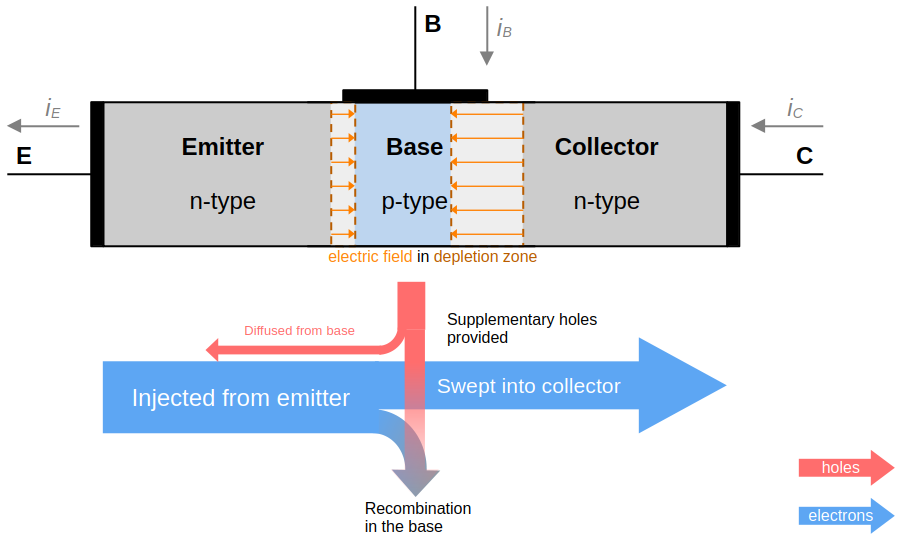
Visualization of the forward active region of a NPN BJT.
💡 We consider the flow of electrons because they are the majority carriers on the emitter and collector terminals. Injection of holes from base to emitter also exist, but remains insignificant as compared to the injection of electrons.
Almost all injected electrons are swept into the collector region, so we can approximate \(i_C \approx i_E\). By the PN junction’s I-V characteristic equation, we can describe \(i_C\) in terms of \(v_{BE}\) as an exponential,
\[i_C = I_S\,\left(\mathrm{e}^{v_{BE} / V_T} - 1\right) \approx I_S\,\mathrm{e}^{v_{BE} / V_T}\]where
- \(I_S\) is the reverse saturation current of the BE junction, and
- \(V_T := k_B T / q\). At room temperature, \(V_T \approx 26\,\mathrm{mV}\).
💡 When operating in the forward active region, \(v_{BE}\) is large, so we drop the \(-I_S\) term.
Something more interesting will happen as we change the voltage of the collector region \(v_{CE}\). The higher \(v_{CE}\) is, the more reverse-biased the BC junction becomes, and the wider its depletion region is. A wider depletion region causes a smaller base effective width, so even fewer electrons recombine in the base region, leading to a larger \(i_C\). This effect is called the Early effect.
Taking into account the Early effect, we can write the complete equation on \(i_C\) as
\[\boxed{i_C = I_S\,\mathrm{e}^{v_{BE} / V_T}\left(1 + \frac{v_{CE}}{V_A}\right)}\]where \(V_A\) is the Early voltage, typically in the range of \(50 \sim 100\,\mathrm{V}\).
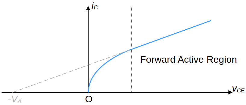
Visualization of the Early effect of a BJT.
In the reverse active region, the biases are the opposite, so the BJT works the other way around: the collector injects electrons into the base, which gets swept into the emitter region.
However, the collector is mildly doped and the emitter is heavily doped, which leads to weaker electron injection and increased difficulty of sweeping electrons into the emitter region, eventually causing smaller current gain. This is suboptimal, so the reverse active region has barely any application.
Saturation and Cutoff
Consider saturation region first, with the BE and BC junctions both forward-biased.
Now, as the injected electrons from the emitter enters the base region, the depletion zone becomes narrower due to the forward-biasing of the BC junction, so less electrons get swept into the collector region. In turn, more electrons will be recombined with holes in the base region, so the supply of holes must be larger. Moreover, since the BC junction is also in forward bias, the collector will start injecting electrons back to the base.
Therefore, in the saturation region,
- \(i_B\) increases, \(i_C\) decreases, leading to reduced gain \(\beta\), and
- the voltage \(v_{CE}\) is small and nearly constant due to forward-biasing.
In the saturation region, the NPN BJT behaves like a closed switch, conducting current from the collector to the emitter.
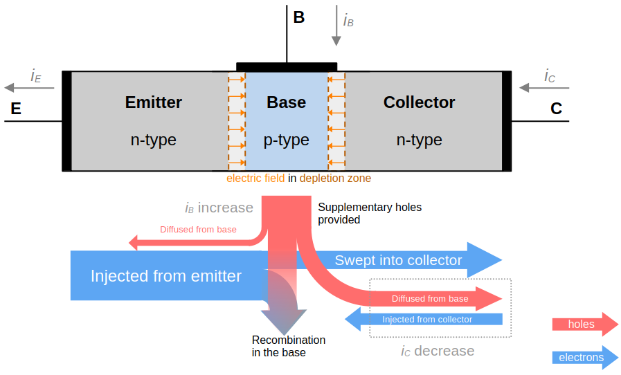
Visualization of the saturation region of a NPN BJT.
In the cutoff region, both junctions are in reverse bias, so there is no significant injection of carriers. The NPN BJT behaves like an open switch, blocking current flow.
PNP BJTs at a Glance
We can also put the n-type material in the middle, and the p-type material on the sides. This configuration is known as a PNP BJT. In a PNP BJT, most principles are similar to a NPN BJT, but
- the majority carrier are holes instead of electrons, and
- all polarities (current direction, junction voltage for a specific region) are reversed.
However, holes (in the valence band) have less mobility than electrons (in the conduction band), so the current gain of a PNP BJT is smaller than that of an NPN BJT under the same conditions. This is the reason why PNP BJTs are less commonly used.
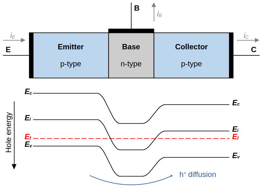
Visualization of a PNP BJT.
BJTs in Circuits
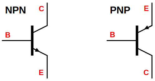
Circuit diagram for NPN and PNP BJTs. The arrow between the base and emitter resembles the polarity of the BE junction.
Now let’s connect the BJTs into a circuit and observe the effects. The governing equations are
\[\boxed{\begin{aligned} i_C &= i_S\,\mathrm{e}^{v_{BE} / V_T}\left(1 + \frac{v_{CE}}{V_A}\right) \\ i_C &= \beta\,i_B \\ i_E &= i_B + i_C \end{aligned}}\]In the discussions below, we will be using NPN BJTs for demonstration.
Voltage Transfer Characteristics
In real-world applications, a BJT is usually connected in a common-emitter configuration, where
- the emitter node is grounded,
- the collector node, used as the output voltage, is connected to a constant voltage source \(V_{CC}\) by a pull-up resistor \(R_C\), and
- the base node is used as the input voltage.
As we increase the input voltage \(v_{B}\), the output voltage \(v_{C}\) curve will behave differently, corresponding to three different operating regions.
- Cutoff: The NPN BJT barely conducts, so \(v_{C}\) can be seen as \(V_{CC}\).
- Forward active: \(i_{C}\) increases exponentially with \(v_{B}\), so \(v_{C}\) decreases due to the increasing voltage drop on the pull-up resistor.
- Saturation: The NPN BJT saturates when \(v_{C}\) drops below \(0.3\,\mathrm{V}\), with \(v_{C}\) nearly constant.
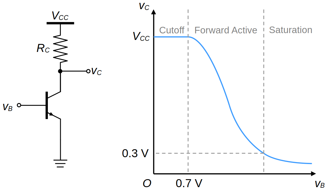
Common-emitter configuration and its voltage transfer characteristics.
We can see that NPN BJT outputs low when input is high, and outputs high when input is low, functioning as an “inverted” digital switch. On the other hand, a PNP BJT outputs high when input is high, and outputs low when input is low, functioning as a “normal” digital switch. This property makes them applicable in digital circuits. But in real life, they are now rarely used due to their
- large power consumption even when not switching because of consistent collector current, and
- limited fanout arising from small but non-negligible base current.
Their roles in digital circuits are largely taken over by MOSFETs.
Small-Signal Analysis
BJTs are often used as common-emitter amplifiers (CE amplifiers) in analog circuits, connected similarly to the figure above. For analysis, the three equations listed at the beginning of this section are sufficient. However, they are nonlinear, and computation will be a disaster if the outer circuit is also complex. Therefore, simplification models are necessary for the ease of computation.
But, in order to simplify the equations, some assumptions need to be made.
Large Signal and Small Signal
When the variation of the signal is large, no approximation can be made appropriately. In this case, we have to use the full nonlinear equation. This signal is called large signal.
However, when the variation of the signal is small, we can make a linear approximation around the point where the signal lies. This point is called the quiescent point (Q-point for short), and the signal itself is called small signal.
When doing small signal analysis, one common method is to split the signal into a DC bias and a small AC component, analyze them separately, and combine the effects using the superposition principle of circuits.
- The DC bias determines the Q-point and ensures operation in the forward active region, while
- the AC component gets amplified by circuit, its gain equal to the slope of the transfer function.
In this post, we use uppercase \(V_C\) to refer to the DC bias, while lowercase \(v_c\) to describe the AC component. The full signal is represented as lowercase symbol with uppercase subscript, \(v_{CE}\).
💡 The superposition principle requires the circuit to be linear, which is not the case for the BJT. However, we are applying it on the linear circuit model approximated at the Q-point, so no worry.
The Hybrid-\(\pi\) Model
The hybrid-\(\pi\) model is essentially the first-order approximation of an NPN BJT in the forward active region given the Q-point. It consists of three circuit elements,
- a voltage-controlled current source (transconductance \(g_m\)) at the collector,
- a resistor \(r_\pi\) between the emitter and base, and
- a resistor \(r_o\) in parallel with the current source.
The parameters are not just magic numbers: they capture characteristic first-order effects of a BJT.
| Parameter | Symbol | Value | Captures |
|---|---|---|---|
| Transconductance | \(g_m\) | \(I_C / V_T\) | electron dynamics from emitter to collector |
| BE resistance | \(r_\pi\) | \(\beta / g_m\) | diode characteristic of the BE junction |
| Output resistance | \(r_o\) | \(V_A / I_C\) | Early effect on collector current with CE voltage |
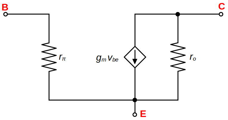
The hybrid-π model's circuit diagram.
Applying the Model
In order to apply the hybrid-\(\pi\) model, the following steps are taken:
- Find the collector current \(I_C\) from the DC bias (determine the Q-point);
- Compute the parameters in the model;
- Analyze the DC bias and AC component separately, then combine using superposition principle.
The CE Amplifier
Core Structure
A CE amplifier is essentially an NPN BJT connected using the common-emitter configuration. It
- works at the Q-point determined by the DC component of \(v_B\), and
- amplifies the AC component of \(v_B\) into \(v_C\).
By the hybrid-\(\pi\) model, we can derive the voltage gain of the small signal as
\[A_v = -g_m (R_C \parallel r_o) = -g_m \frac{R_C\,r_o}{R_C + r_o}\]Since the output resistance coming from the Early effect is large, typically the gain can be further rounded to \(A_v \approx -g_m R_C\) without being too far off.
However, this setup is not optimal due to several reasons, including
- Unreliableness of DC component: we cannot guarantee that the DC component of the input voltage is stable enough; and
- Sensitivity of gain: a small fluctuation in either base voltage (affecting \(v_{BE}\)) or temperature (affecting \(V_T\)) results in a large change in \(i_C\), thus affecting gain.
These factors will cause significant non-linear effects even for a small AC component. So optimizations are needed, and we can approach the problem from three perspectives.
Optimizations
Input Optimization: AC Coupling
We cannot rely on the DC component of the input voltage, which makes our life a bit hard. But look, we have a stable DC voltage source \(V_{CC}\) at hand. So let’s divide the voltage of \(V_{CC}\) by two resistors and use that as the DC bias for the BJT. Then, we can simply couple the AC component of the input signal onto that DC bias.
How can we do that? Think of capacitors: they block DC and allow AC passage. Therefore, we can take a capacitor, connect one end to the input signal, and feed the other end into \(v_{B}\). By the superposition principle, \(v_B\) will now receive a DC component from the division of \(V_{CC}\) which is stable, and an AC component from the input signal. Done!
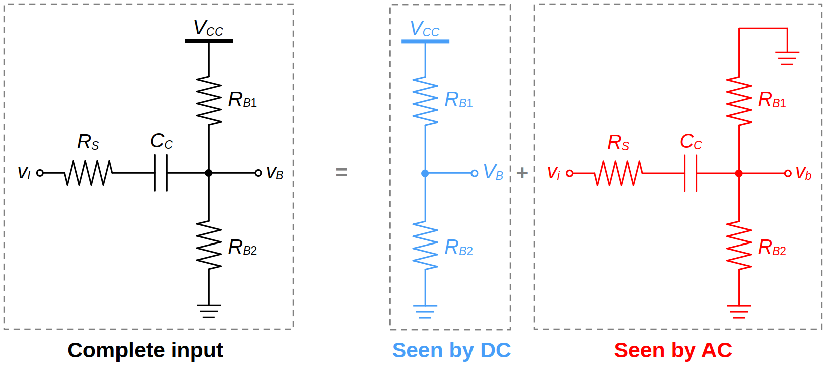
Visualization of input AC coupling.
💡 Caution: when analyzing the AC component, the pull-up resistor should be tied to the ground, because the constant voltage source \(V_{CC}\) is turned off for AC analysis.
BJT Optimization: Emitter Degeneration
The problem with the sensitivity of the gain lies in the exponential relationship \(i_C \propto \mathrm{e}^{v_{BE} / V_{T}}\), making voltage fluctuations incredibly difficult to harness. An operational amplifier is similar: its open-loop gain is also very large and hard to control. However, by feeding the output back to the inverting terminal of an op-amp, the huge open-loop gain can be tampered and used in negative-feedback regulation. Can we do something similar here?
Absolutely! In a naked CE amplifier, the emitter is hard-wired to the ground, so it cannot adapt dynamically to the fluctuation in the base voltage. So in response, we connect a pull-down resistor \(R_E\) between the emitter node and the ground. Let’s see what happens when we increase the collector current \(I_C\) a little.
- \(I_C\) increases, causing
- the voltage drop \(I_CR_E\) on the pull-down resistor to rise, which results in
- a decrease of the junction voltage \(V_{BE}\), and finally leads to
- a drop in \(I_C\).
When \(I_C\) dips down, the mechanism is similar. Therefore, by adding a pull-down resistor on the emitter, we can achieve a negative-feedback regulation on \(I_C\), which leads to a better linear effect. This is called emitter degeneration.
But this optimization comes at a cost: the voltage gain will decrease. Circuit analysis reveals the reduced gain to be (small terms omitted)
\[A_v = \frac{-g_m R_C}{1 + g_m R_E}\]and if the term \(g_m R_E\) is large enough, the gain becomes \(A_v \approx -R_C / R_E\), which is completely independent of the BJT itself, eliminating the impact of errors on \(\beta\) during manufacture.
Key parameters before and after emitter degeneration are derived from small signal analysis.
| Parameter | Expression | Before degeneration | After degeneration |
|---|---|---|---|
| Voltage gain \(A_v\) | \(v_c / v_b\) | \(-g_m(R_C\parallel r_o)\approx -g_mR_C\) | \(\frac{-g_mR_C}{1+g_mR_E}\approx -\frac{R_C}{R_E}\) |
| Current gain \(A_i\) | \(i_c / i_b\) | \(\beta\) | \(\beta\) |
| Input impedance \(r_\text{in}\) | \(v_b / i_b\) | \(r_\pi\) | \(r_\pi + (\beta + 1)R_E\) |
| Output impedance \(r_\text{out}\) | \(v_c / i_c\) | \(R_C\) | \(R_C\) |
The regulation is targeted mainly at the DC component but not AC, but a simple pull-down resistor affects both DC and AC. To minimize this trade-off, we can connect a capacitor \(C_E\) in parallel with \(R_E\), allowing the AC component to bypass it in order to increase its gain. For more finer control, we can even divide \(R_E\) into two parts and connect \(C_E\) in parallel with only one of them.
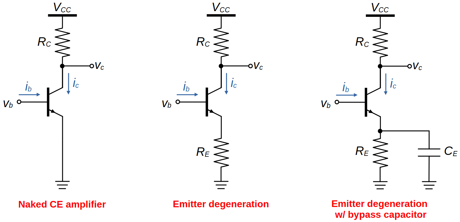
Visualization of emitter degeneration with bypass capacitor.
Load Optimization: Capacitor Coupling
Real transistors rarely operate individually. As a result, there is a need for the output of one CE amplifier to drive a load or another CE amplifier at the next stage, which typically requires only the AC component at the output. Therefore, another coupling capacitor is often connected at the collector terminal before the actual output to remove the DC component of the output signal.
Complete Structure
With the above three optimizations, we have successfully upgraded an unstable BJT amplifier into a full-blown, robust CE amplifier. It now
- achieves stable performance by coupling the input’s AC component onto the DC bias generated by dividing \(V_{CC}\) voltage,
- creates externally-manageable gain by emitter degeneration, and
- allows for multi-level connection by capacitor coupling on the output terminal.
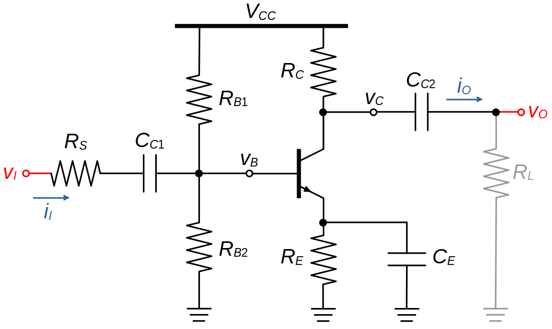
The complete CE amplifier circuit.
Summary
In our expedition into BJTs, we have seen what amazing characteristics the BJT’s coupling effects can produce, which is a lot more interesting than simply two diodes connected back-to-back. Its small-signal properties when connected into a circuit are also intriguing, making BJTs a cornerstone in modern analog circuits with wide application in CE amplifiers.
References
- Lecture slides from the Ve311 course in Summer 2026, taught by Prof. Xuyang Lu (卢旭阳).
Note: BJT stands for “Bipolar Junction Transistor” in this text, not “Business Japanese Test.” But anyway, if you’re indeed taking the exam, I wish you pass with flying colors. 🌟