Semiconductor Physics: From Silicon To Diodes
 2026-05-27
  electronics, semiconductor, notes
This is a summary note of the semiconductor physics part in the course “Ve311 Electronic Circuits,” introducing the basic working principles of a PN junction from the atomic fundamentals.
Note: You may view the Chinese translation of the post here, but it is only for reference.
Quantum View of Silicon
Valence and Conduction Bands
Silicon has an atomic number of 14, and its electron configuration is given by \([\text{Ne}]3\text{s}^2 3\text{p}^2\). In an isolated silicon atom, the electrons’ wavefunctions and energy levels are cleanly quantized and discrete, so there are no special effects worth attention.
However, in a silicon crystal where the interatomic distance is comparable to the size of atoms, the wavefunctions of different silicon atoms overlap significantly. This will lead to merging and recombination, and the net result is
- a valence band at the lower energies, and
- a conduction band at the higher energies.
A band is an energy region containing many possible energy levels.
Between the valence band and the conduction band, there is a bandgap, in which there are no energy levels existing. The size of the bandgap is measured by the energy difference between the two bands, typically denoted as \(E_g\). For silicon, \(E_g = 1.12\,e\mathrm{V}\) at room temperature.
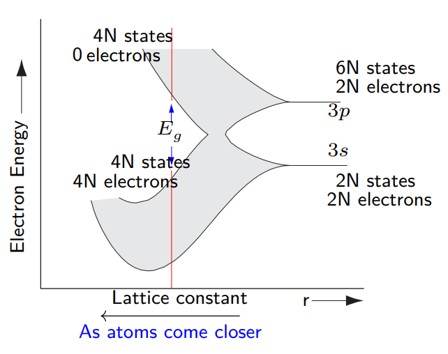
Visualization of two bands and bandgap. (Picture taken from lecture slides)
Electrons and Holes
At \(0\,\text{K}\), the valence band is completely filled, and the conduction band is completely empty.
As temperature gradually increases, some electrons will be excited and enter the conduction band, leaving behind holes in the valence band. The negatively charged electrons can move freely in the conduction band, and the positively charged holes can also “move” freely in the valence band, so they both act as current carriers, called intrinsic carriers, whose concentration is denoted as \(n_i\).
💡 Actually, in the valence band, it is still the electrons that are actually moving, occupying holes and leaving behind new ones. However, that is difficult to describe quantitatively. Therefore, the equivalent description using holes is used.
Let’s consider electrons first. To quantify the distribution of electrons in the two bands, we need two important characteristics,
- the quantum state density \(g_c(E)\) and \(g_v(E)\), which is the number of available quantum states per unit volume per unit energy at energy level \(E\), and
- the distribution function \(f(E)\), which is the probability that a specific quantum state with energy \(E\) is occupied by an electron.
Electrons are fermions that obey the Pauli Exclusion Principle, so they are described by the Fermi-Dirac distribution function as follows,
\[f(E) = \frac{1}{1 + \exp\left(\frac{E - E_f}{k_BT}\right)}\]where:
- \(T\) is the absolute temperature,
- \(k_B\) is the Boltzmann constant \(8.62 \times 10^{-5}\,e\mathrm{V\cdot K^{-1}}\), and
- \(E_f\) is the Fermi level, which is an energy reference that reflects the electric potential of electrons. It is also a statistical description, measuring the 50% point of the Fermi-Dirac distribution. There does not necessarily exist an energy level that is exactly at \(E_f\).
The electron concentration \(n\) in the conduction band is thus given by the integration
\[n = \int_{E_c}^\infty g_c(E) f(E) \mathrm{d}E\]For the hole concentration \(p\) in the valence band, we need to use \(1 - f(E)\) which is the probability that a specific quantum state is NOT occupied by an electron,
\[p = \int_{-\infty}^{E_v} g_v(E) (1 - f(E)) \mathrm{d}E\]For intrinsic (pure) silicon, the generation of an electron always comes with the generation of a hole, so we have \(n = p = n_i\), which further implies that the Fermi level sits in the middle of the bandgap, denoted as the intrinsic Fermi level \(E_i\).
The integration, on the other hand, yields an important, general relation,
\[\boxed{n_i^2 = np = BT^3\exp\left(-\frac{E_g}{k_BT}\right)}\]where \(B\) is a material-dependent constant. For silicon, \(B = 1.08 \times 10^{31}\,\mathrm{K^{-3}\cdot cm^{-6}}\). The equation \(n_i^2 = np\) describes a balance in electron and hole concentrations adjusted by pairing, while the \(BT^3\exp\) term quantifies how much carriers in total can be generated under the specific conditions.
💡 Quick calculation: At room temperature \(300\,\text{K}\), \(n_i \approx 10^{10}\,\mathrm{cm^{-3}}\) for intrinsic silicon, which is small compared to the atom concentration. Therefore, pure silicon is a poor conductor.
Doping
Meaning of Doping
Since pure silicon conducts poorly, we need to introduce additional carriers into the system. There are two types of materials worth considering, including
- electron donor atoms that has 1 electron more in the valence shell, such as phosphorus, and
- electron acceptor atoms that has 1 electron less (equivalent to 1 hole more) in the valence shell, such as boron.
When donors are more than acceptors, the electron concentration \(n\) will increase and become the majority carrier, so it is called n-type doping. Otherwise, the hole concentration \(p\) will increase and become the majority carrier, called p-type doping.
Realistic Doping Calculation
In realistic doping, the introduced donors and acceptors are large in quantity, so it is safe to assume
- full ionization, meaning that the concentration of additional carriers is equal to the concentration of the dopant, and
- the concentrations of majority carriers and additional carriers are equal.
Take a simple n-type doping as example: if the dopant concentration is \(N_D\) (\(N_D \gg n_i\)), the concentration of additional electrons by the introduction of the dopant is \(N_D^+\), and the final concentration of electrons (majority carrier) is \(n\), then we can safely assume \(N_D = N_D^+ = n\). Then the minority carrier concentration can be derived from \(np = n_i^2\).
💡 Think of the autoprotolysis equilibrium of water. The approximations here are similar to those used in the calculations involving acid and base solutions.
Energy Level Changes
The introduction of dopants will shift the position of the Fermi level. In n-type doping, there are more electrons in the conduction band, so the probability of electron occupation in the conduction band will become larger, leading to a increase in the Fermi level. In p-type doping, vice versa.
The quantitative equations are, with \(q = e\) being the carrier charge,
\[\boxed{\begin{aligned} q \phi_n &= E_f - E_i = k_BT\ln\left(\frac{n}{n_i}\right) & \text{(n-type)} \\ q \phi_p &= E_i - E_f = k_BT\ln\left(\frac{p}{n_i}\right) & \text{(p-type)} \end{aligned}}\]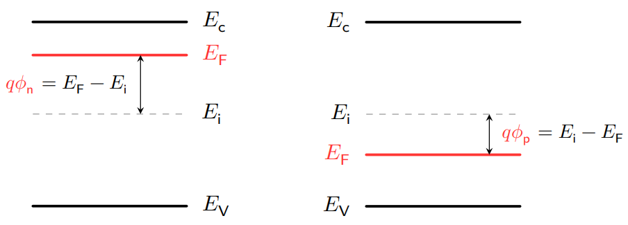
Visualization of Fermi level change, n-type left, p-type right. (Picture taken from lecture slides)
The PN Junction
An isolated block of doped material is boring. The real fun begins when two blocks of p-type and n-type doped materials come into intimate contact, known as a PN junction.
Diffusion and Drift
Two characteristic factors interact in a PN junction:
- diffusion of majority carriers, and
- drift of minority carriers.
When the PN junction is in equilibrium (no external voltage applied), diffusion and drift balance each other, causing no net flow of current.
From the Dynamics Perspective
The p-type material contains high concentration of holes but low concentration of electrons. The n-type material, on the other hand, contains high concentration of electrons but low concentration of holes. Given this concentration difference, diffusion of majority carriers will occur as long as the materials are in intimate contact:
- Electrons will enter the p-side from the n-side. On their entrance, they will come in contact with an excess of holes and pair with them, charges neutralizing. Left behind by the diffused electrons are ionized, fixed n-type dopants with a net positive charge;
- Holes will enter the n-side from the p-side. On their entrance, they will come in contact with an excess of electrons and pair with them, charges also neutralizing. Left behind by the diffused holes are ionized, fixed p-type dopants with a net negative charge.
The net diffusion current is from the p-side to the n-side. This diffusion process will produce a depletion zone with no freely-moving majority carriers at the surface of contact, with positive charge in the n-side and negative charge in the p-side. The charge distribution will thus create an internal electric field, pointing from the n-side to the p-side, blocking further diffusion.
The electric field further induces drift of minority carriers. P-side electrons drift towards the n-side, while n-side holes drift towards the p-side, resulting in a drift current from the n-side to the p-side. This drift current is limited by the concentration of minority charges, so changes in the internal electric field will not alter it significantly.
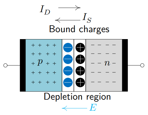
Visualization of diffusion (D) and drift (S) from the dynamics perspective. (Picture taken from lecture slides)
💡 Majority carriers diffuse due to concentration difference \(\implies\) Depletion zone & internal electric field \(\implies\) Minority carriers drift due to electric field \(\implies\) zero net current.
From the Energy Perspective
The Fermi level of a block of material measures the electric potential of its electrons. Since there is no net current in the PN junction at equilibrium, the Fermi level of the p-side and n-side should match.
In order to achieve this aim, the energy levels of the p-side increase, while the energy levels of the n-side decrease, resulting in an potential barrier referred to as the built-in potential,
\[\boxed{\phi_i = \phi_p + \phi_n = \frac{k_BT}{q}\ln\left(\frac{N_AN_D}{n_i^2}\right)}\]where \(N_A\) and \(N_D\) are the concentration of dopants on the p-side and n-side respectively. This potential barrier will be seen by the diffusing majority carriers, thus blocking its flow.
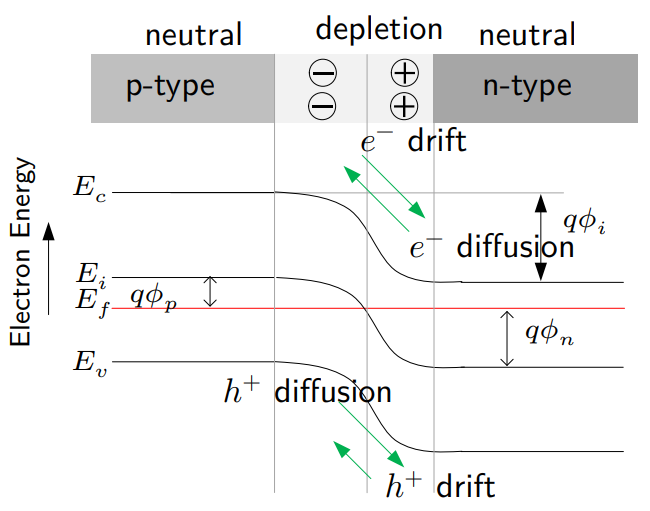
Visualization of the built-in potential from the energy perspective. (Picture taken from lecture slides)
Applying External Voltage
A PN junction can serve as a diode when connected into a circuit, regulating current to flow in only one direction. To begin with, we shall discuss how the PN junction behaves when an external voltage \(V_a\) is applied to it. There are two ways:
- p-side seeing higher potential, referred to as forward bias, and
- n-side seeing higher potential, referred to as reverse bias.
Forward Bias and Reverse Bias
When the p-side of the PN junction sees higher potential (forward bias), its Fermi level drops due to electrons being drawn away by the voltage source. On the other hand, the n-side sees lower potential, accepts electrons shoved into it by the voltage source, and its Fermi level rises. Therefore, the potential barrier is reduced to \(\phi_i - V_a\) and the depletion zone narrows, which in turn lead to a significant increase in diffusion current. The net result is a large forward current carried by the diffusing majority carriers in the PN junction.
When the n-side of the PN junction sees higher potential (reverse bias), its Fermi level rises, and conversely, the Fermi level of the p-side drops. The potential barrier is hence increased to \(\phi_i + V_a\) with depletion zone widening, which blocks diffusion even further. The net result is a small reverse current carried by the drifting minority carriers in the PN junction.
The current in the PN junction given a voltage bias \(V_a\) is
\[\boxed{I_D = I_S\left(\mathrm{e}^{\frac{qV_a}{k_BT}} - 1\right)}\]where \(I_S\) is the reverse saturation current, which is essentially the drift current described earlier.
💡 It can be observed that when \(V_a\) is positive the diode current \(I_D\) increases dramatically due to the exponential. Therefore, putting a diode in forward bias without a resistor in series should always be avoided.
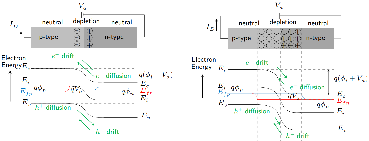
Visualization of forward (left) and reverse (right) bias. (Picture taken from lecture slides)
Reverse Breakdown
Reverse bias cannot increase limitlessly. When the reverse bias voltage exceeds a certain threshold \(V_{BR}\), the PN junction will see an enormous increase in reverse current, meaning that it ceases to restrict current to flow in only one direction. This phenomenon is called breakdown.
There are two mechanisms of breakdown, avalanche breakdown and Zener breakdown.
- Avalanche breakdown: The reverse bias voltage is so high that a free electron gains enough energy to “knock” another valence electron into the conducting band on collision, thus creating a new electron-hole pair, which can further create more electron-hole pairs after acceleration and collision with other electrons, finally resulting in a chain reaction and causing an “avalanche” of newly-created charge carriers that produces a large current. Avalanche breakdown is typically hard to control, so it is not expected and even unfavorable in most scenarios.
- Zener breakdown: The reverse bias causes electrons to “tunnel through” the bandgap, directly jumping from the valence band to the conduction band without requiring the kinetic energy needed to cross the potential barrier. This is a quantum-mechanical effect, and typically happens to heavily-doped PN junctions with a very narrow depletion zone. Unlike avalanche breakdown, Zener breakdown has a nearly constant reverse breakdown voltage, making it easy to harness, so it is utilized to design and manufacture voltage regulators.
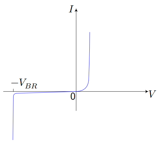
I-V characteristics of a PN junction, including reverse breakdown. (Picture taken from lecture slides)
Summary
Presented above is a complete story from the physical properties of silicon to the usage of PN junctions. Silicon crystals provide separate valence and conduction bands, doping increases carrier concentration, and PN junction makes use of diffusion and drift between two types of doping. PN junctions can serve as diodes, and they are the backbone of all electronic circuits used today.
References
- Lecture slides from the Ve311 course in Summer 2026, taught by Prof. Xuyang Lu (卢旭阳).