<?xml version="1.0" encoding="utf-8"?><feed xmlns="http://www.w3.org/2005/Atom" ><generator uri="https://jekyllrb.com/" version="3.10.0">Jekyll</generator><link href="https://tomategg-101325.github.io/feed.xml" rel="self" type="application/atom+xml" /><link href="https://tomategg-101325.github.io/" rel="alternate" type="text/html" /><updated>2026-06-27T10:20:03+00:00</updated><id>https://tomategg-101325.github.io/feed.xml</id><title type="html">番茄炒蛋 🍅🥚</title><subtitle>一个有趣的家伙的个人网站 :P</subtitle><entry><title type="html">数据结构课程 Project 3 重写记</title><link href="https://tomategg-101325.github.io/zh-cn/2026/06/27/ve280-p3-reformation-cn.html" rel="alternate" type="text/html" title="数据结构课程 Project 3 重写记" /><published>2026-06-27T02:00:00+00:00</published><updated>2026-06-27T02:00:00+00:00</updated><id>https://tomategg-101325.github.io/zh-cn/2026/06/27/ve280-p3-reformation-cn</id><content type="html" xml:base="https://tomategg-101325.github.io/zh-cn/2026/06/27/ve280-p3-reformation-cn.html"><![CDATA[<p>事情是这样的：我这学期在上一门数据结构的课程，虽然感觉难度不大，但是它的 Project 3 一堆条条框框，让我写得非常不爽；于是在<em>按照要求做完提交</em>之后，我又抽时间自己从零搭了一个能实现一模一样功能的程序，但是除了使用 C++17 标准之外<strong>完全不设任何限制</strong>。最后我做出了一个用<strong>回调函数实现解耦</strong>的架构。写这篇帖子是简要介绍一下我是<strong>如何搓出这个架构</strong>的。</p>

<p>重写过的项目源码在<a href="https://github.com/tomategg-101325/species-simulator">这里</a>，实现的功能也写在 readme 里面了，这里不做过多赘述。简而言之，就是一个<strong>高度可扩展的物种演化模拟程序</strong>。</p>

<p>You can view the English translation of the post <a href="/en-us/2026/06/27/ve280-p3-reformation-en.html">here</a>, but it is only for reference.</p>

<h2 id="痛点模拟器层次的复杂度">痛点：模拟器层次的复杂度</h2>

<p>由于项目要求限制<sup id="fnref:1" role="doc-noteref"><a href="#fn:1" class="footnote" rel="footnote">1</a></sup>，在交上去的代码里，模拟器层次有一个巨大的 <code class="language-plaintext highlighter-rouge">switch</code> 语句块，用来根据物种程序的指令类型来让底下的引擎执行不同的物理操作。下面是代码片段 (不完全是提交上去的代码，但是功能和结构一致)：</p>

<div class="language-cpp highlighter-rouge"><div class="highlight"><pre class="highlight"><code><span class="kt">void</span> <span class="n">Simulator</span><span class="o">::</span><span class="n">SimulateCreature</span><span class="p">(</span><span class="kt">unsigned</span> <span class="kt">int</span> <span class="n">creature_index</span><span class="p">)</span> <span class="p">{</span>
  <span class="p">...</span>
  <span class="n">current_instruction</span> <span class="o">=</span> <span class="n">engine_</span><span class="p">.</span><span class="n">get_instruction</span><span class="p">(</span><span class="n">creature_index</span><span class="p">);</span>  <span class="c1">// obtain current instruction</span>
  <span class="p">...</span>
  <span class="k">switch</span> <span class="p">(</span><span class="n">current_instruction</span><span class="p">.</span><span class="n">opcode</span><span class="p">)</span> <span class="p">{</span>
    <span class="k">case</span> <span class="n">Opcode</span><span class="o">::</span><span class="n">kHop</span><span class="p">:</span>  <span class="c1">// hop forward</span>
      <span class="n">engine_</span><span class="p">.</span><span class="n">MoveCreature</span><span class="p">(</span><span class="n">creature_index</span><span class="p">);</span>
      <span class="k">break</span><span class="p">;</span>
    <span class="k">case</span> <span class="n">Opcode</span><span class="o">::</span><span class="n">kLeft</span><span class="p">:</span>  <span class="c1">// turn left</span>
      <span class="n">engine_</span><span class="p">.</span><span class="n">TurnCreatureLeft</span><span class="p">(</span><span class="n">creature_index</span><span class="p">);</span>
      <span class="k">break</span><span class="p">;</span>
    <span class="p">...</span>
  <span class="p">}</span>
  <span class="p">...</span>
<span class="p">}</span>
</code></pre></div></div>

<p>功能上虽然没有问题，但是这种做法的缺点有不少：</p>

<ul>
  <li>单个函数体<strong>过于复杂</strong>；</li>
  <li>如果将来要增加新的指令，需要再往这个 <code class="language-plaintext highlighter-rouge">switch</code> 里面增添东西，更加<strong>难以维护</strong>；</li>
  <li>指令类型区分和指令执行全部耦合在一起，<strong>调试不方便</strong>。</li>
</ul>

<p>事实上我本地的 code quality 工具直接警告这个 <code class="language-plaintext highlighter-rouge">switch</code> 语句块所在的函数复杂度过高，所幸评测机没卡这个点扣我分。</p>

<p>但为什么一开始会把指令执行放在模拟器里面呢？因为引擎归模拟器管理，而指令的执行又依赖于引擎提供的各种物理操作（例如前进、左转、感染前方生物等等）。</p>

<h2 id="联想嵌入式开发中学到的回调函数">联想：嵌入式开发中学到的回调函数</h2>

<p>在当初写完这个函数之后，我也一直在想能不能把指令执行从模拟器里面<strong>解耦</strong>出去。</p>

<p>某天洗澡的时候，我忽然回忆起嵌入式开发中学到的<strong>回调函数 (callback function)</strong>。回调函数一般是和<strong>中断 (interrupt)</strong> 搭配使用，用来在某个特定的事件发生时对其进行处理。老师教的基本架构是这样：</p>

<ul>
  <li>回调函数层：
    <ul>
      <li>规定一个<strong>函数类型 (function type)</strong>，即函数的参数类型和个数以及函数的返回类型，<em>不包括参数名称、函数名称和具体实现</em>；</li>
      <li>开辟一个该类型函数的<strong>函数指针</strong>的数组作为<strong>注册表 (registry)</strong>；</li>
      <li>提供注册函数的<strong>接口</strong>以及执行所有已注册函数的接口。</li>
    </ul>
  </li>
  <li>应用层：
    <ul>
      <li><strong>实现</strong>具体的事件处理函数，要满足规定的函数类型；</li>
      <li>将处理函数的函数指针<strong>注册</strong>进回调函数层；</li>
      <li>在中断函数里直接<strong>调用</strong>回调函数层给的执行接口。</li>
    </ul>
  </li>
</ul>

<blockquote>
  <p>💡 在嵌入式领域，中断是实现事件处理的方式之一。当某个事件发生的时候，对应的设备会让单片机 (MCU) 知晓，这个时候单片机会中断正在执行的其他程序，转而处理这个刚刚发生的事件。</p>
</blockquote>

<p>这种架构能让回调函数层完全不用知晓应用层要干什么，它只机械地执行应用层传过来的回调函数，因而在需求发生变更时也不用改动。这就是一种解耦的方式。</p>

<h2 id="解决依赖倒置">解决：依赖倒置</h2>

<p>在上述的架构中，回调函数层不依赖于应用层的具体实现，而它俩都依赖于回调函数的<strong>函数类型</strong>。这就是<strong>依赖倒置原理 (Dependency Inversion Principle)</strong>。它要求：</p>

<blockquote>
  <p>高层次不应依赖于低层次；两者都应<strong>依赖于某个抽象 (abstraction)</strong>。</p>

  <p>抽象不应依赖于实现细节；相反，<strong>实现细节应依赖于这个抽象</strong>。</p>
</blockquote>

<p>在嵌入式的例子里，<strong>回调函数的函数类型就是这个抽象</strong>。而稍微迁移一下，依赖倒置原理也能应用在这个项目中。我是这样做的：</p>

<ul>
  <li>抽象出一个<strong>回调函数列表</strong> <code class="language-plaintext highlighter-rouge">WorldCallbacks</code>，包含各种基本的物理操作（获取、设置、判断）；</li>
  <li>抽象出一个执行方法的抽象类 <code class="language-plaintext highlighter-rouge">IMethod</code>，重载其括号运算符用于具体执行，接受上面的这个回调函数列表作为参数，同时让其为虚函数；</li>
  <li>从执行方法的抽象类中继承出具体的各种动作 (action) 和感知 (sensor)，实现具体的执行过程。</li>
  <li>在模拟器里维护一个 <code class="language-plaintext highlighter-rouge">IMethod</code> 类型的指针哈希表，指令名称作为其键值，方便快速调用。</li>
  <li>让引擎提供 <code class="language-plaintext highlighter-rouge">WorldCallbacks</code> 的具体实现。</li>
</ul>

<p>这个回调函数列表就是统一的抽象，模拟器层次和引擎层次都依赖于它。现在，在模拟器的执行逻辑里，只需要根据指令名称定位到对应的执行方法，然后调用其括号运算符，传入准备好的回调函数列表和其他相关参数即可。逻辑简单很多，如果要扩展的话也可以直接继承出一个新的执行类。</p>

<div class="language-cpp highlighter-rouge"><div class="highlight"><pre class="highlight"><code><span class="kt">void</span> <span class="n">Simulator</span><span class="o">::</span><span class="n">SimulateCreature</span><span class="p">(</span><span class="kt">unsigned</span> <span class="kt">int</span> <span class="n">creature_index</span><span class="p">)</span> <span class="p">{</span>
  <span class="p">...</span>
  <span class="n">current_instruction</span> <span class="o">=</span> <span class="n">engine_</span><span class="p">.</span><span class="n">get_instruction</span><span class="p">(</span><span class="n">creature_index</span><span class="p">);</span>  <span class="c1">// obtain current instruction</span>
  <span class="p">...</span>
  <span class="n">std</span><span class="o">::</span><span class="n">shared_ptr</span><span class="o">&lt;</span><span class="n">IMethod</span><span class="o">&gt;</span> <span class="n">executor</span> <span class="o">=</span> <span class="n">get_executor</span><span class="p">(</span><span class="n">current_instruction</span><span class="p">.</span><span class="n">opcode</span><span class="p">);</span>  <span class="c1">// obtain executor</span>
  <span class="p">...</span>
  <span class="p">(</span><span class="o">*</span><span class="n">executor</span><span class="p">)(</span><span class="n">world_callbacks</span><span class="p">,</span> <span class="n">creature_index</span><span class="p">,</span> <span class="p">...);</span>  <span class="c1">// dispatch the executor</span>
  <span class="p">...</span>
<span class="p">}</span>
</code></pre></div></div>

<p>重写过的这个 <code class="language-plaintext highlighter-rouge">SimulateCreature</code> 函数虽然看上去还会很复杂，但是其核心就是上面的这三行代码：<strong>获取指令、找到执行方法，传入参数执行</strong>。其它的都是一些检查判断之类的操作，是为了满足杂七杂八的其他需求。如果后续还要加新的功能的话，是<strong>完全不用动它</strong>的。</p>

<h2 id="脚注">脚注</h2>

<div class="footnotes" role="doc-endnotes">
  <ol>
    <li id="fn:1" role="doc-endnote">
      <p>连头文件都要用白名单限制是何意味呢我请问了？连 <code class="language-plaintext highlighter-rouge">stdexcept</code> 和 <code class="language-plaintext highlighter-rouge">memory</code> 都不让引，害得我抛个异常都得用字符串字面量 (string literal)，智能指针也用不了，相当的不优雅…… <a href="#fnref:1" class="reversefootnote" role="doc-backlink">&#8617;</a></p>
    </li>
  </ol>
</div>]]></content><author><name></name></author><category term="zh-cn" /><category term="programming" /><category term="cpp" /><category term="notes" /><summary type="html"><![CDATA[事情是这样的：我这学期在上一门数据结构的课程，虽然感觉难度不大，但是它的 Project 3 一堆条条框框，让我写得非常不爽；于是在按照要求做完提交之后，我又抽时间自己从零搭了一个能实现一模一样功能的程序，但是除了使用 C++17 标准之外完全不设任何限制。最后我做出了一个用回调函数实现解耦的架构。写这篇帖子是简要介绍一下我是如何搓出这个架构的。]]></summary></entry><entry><title type="html">Rewriting Data Structures Course Project 3</title><link href="https://tomategg-101325.github.io/en-us/2026/06/27/ve280-p3-reformation-en.html" rel="alternate" type="text/html" title="Rewriting Data Structures Course Project 3" /><published>2026-06-27T02:00:00+00:00</published><updated>2026-06-27T02:00:00+00:00</updated><id>https://tomategg-101325.github.io/en-us/2026/06/27/ve280-p3-reformation-en</id><content type="html" xml:base="https://tomategg-101325.github.io/en-us/2026/06/27/ve280-p3-reformation-en.html"><![CDATA[<p>Here’s the story: I’m taking a data structures course this semester. Although I don’t find it particularly difficult, Project 3 came with so many restrictive rules and constraints that it made me quite frustrated. So after <em>submitting the required version</em>, I took some extra time to rebuild a program from scratch that implements exactly the same functionality, but with <strong>no restrictions whatsoever</strong>—except for using C++17. In the end, I came up with an architecture that uses <strong>callback functions for decoupling</strong>. This post is a brief introduction to <strong>how I built this architecture</strong>.</p>

<p><a href="https://github.com/tomategg-101325/species-simulator">Here</a> is the source code for the rewritten version. Since the functionality is also described in the readme, I won’t go into too much detail here. In short, it’s a <strong>highly extensible species evolution simulation program</strong>.</p>

<p>Note: This post is a translated version. See <a href="/zh-cn/2026/06/27/ve280-p3-reformation-cn.html">here</a> for the original content.</p>

<h2 id="pain-point-complexity-in-the-simulator-layer">Pain Point: Complexity in the Simulator Layer</h2>

<p>Due to the project requirements<sup id="fnref:1" role="doc-noteref"><a href="#fn:1" class="footnote" rel="footnote">1</a></sup>, in the submitted code, the simulator layer had a huge <code class="language-plaintext highlighter-rouge">switch</code> statement block that directed the underlying engine to perform different physical operations based on the instruction type of the creature program. Below is a code snippet (not exactly the submitted code, but the functionality and structure are identical):</p>

<div class="language-cpp highlighter-rouge"><div class="highlight"><pre class="highlight"><code><span class="kt">void</span> <span class="n">Simulator</span><span class="o">::</span><span class="n">SimulateCreature</span><span class="p">(</span><span class="kt">unsigned</span> <span class="kt">int</span> <span class="n">creature_index</span><span class="p">)</span> <span class="p">{</span>
  <span class="p">...</span>
  <span class="n">current_instruction</span> <span class="o">=</span> <span class="n">engine_</span><span class="p">.</span><span class="n">get_instruction</span><span class="p">(</span><span class="n">creature_index</span><span class="p">);</span>  <span class="c1">// obtain current instruction</span>
  <span class="p">...</span>
  <span class="k">switch</span> <span class="p">(</span><span class="n">current_instruction</span><span class="p">.</span><span class="n">opcode</span><span class="p">)</span> <span class="p">{</span>
    <span class="k">case</span> <span class="n">Opcode</span><span class="o">::</span><span class="n">kHop</span><span class="p">:</span>  <span class="c1">// hop forward</span>
      <span class="n">engine_</span><span class="p">.</span><span class="n">MoveCreature</span><span class="p">(</span><span class="n">creature_index</span><span class="p">);</span>
      <span class="k">break</span><span class="p">;</span>
    <span class="k">case</span> <span class="n">Opcode</span><span class="o">::</span><span class="n">kLeft</span><span class="p">:</span>  <span class="c1">// turn left</span>
      <span class="n">engine_</span><span class="p">.</span><span class="n">TurnCreatureLeft</span><span class="p">(</span><span class="n">creature_index</span><span class="p">);</span>
      <span class="k">break</span><span class="p">;</span>
    <span class="p">...</span>
  <span class="p">}</span>
  <span class="p">...</span>
<span class="p">}</span>
</code></pre></div></div>

<p>Functionally, this works fine, but it has several drawbacks:</p>

<ul>
  <li>The single function body is <strong>overly complex</strong>;</li>
  <li>Adding new instructions in the future would require modifying this <code class="language-plaintext highlighter-rouge">switch</code> block, making it <strong>harder to maintain</strong>;</li>
  <li>Instruction type discrimination and instruction execution are all coupled together, which <strong>makes debugging inconvenient</strong>.</li>
</ul>

<p>In fact, my local code quality tool directly warned that the function containing this <code class="language-plaintext highlighter-rouge">switch</code> block had excessive complexity. Fortunately, the online judge didn’t give me a deduction for that.</p>

<p>But why was instruction execution placed inside the simulator in the first place? Because the engine is managed by the simulator, and the execution of instructions depends on various physical operations provided by the engine (e.g., moving forward, turning left, infecting the creature ahead, etc.).</p>

<h2 id="association-callback-functions-learned-in-embedded-development">Association: Callback Functions Learned in Embedded Development</h2>

<p>After I finished writing that function, I kept thinking about whether I could <strong>decouple</strong> instruction execution from the simulator.</p>

<p>One day while showering, I suddenly recalled <strong>callback functions</strong> learnt from embedded development. Callbacks are typically used with <strong>interrupts</strong> to handle specific events when they occur. The basic architecture taught by the teacher was:</p>

<ul>
  <li>Callback layer:
    <ul>
      <li>Define a <strong>function type</strong> (i.e., the parameter types, count, and return type of the function), <em>excluding parameter names, function name, and concrete implementation</em>;</li>
      <li>Declare an array of <strong>function pointers</strong> of that type as a <strong>registry</strong>;</li>
      <li>Provide an <strong>interface</strong> for registering functions and an interface for executing all registered functions.</li>
    </ul>
  </li>
  <li>Application layer:
    <ul>
      <li><strong>Implement</strong> the concrete event handlers, ensuring they conform to the specified function type;</li>
      <li><strong>Register</strong> the function pointers of these handlers into the callback layer;</li>
      <li>Inside the interrupt service routine, simply <strong>call</strong> the execution interface provided by the callback layer.</li>
    </ul>
  </li>
</ul>

<blockquote>
  <p>💡 In embedded systems, interrupts are one way to handle events. When an event occurs, the corresponding device notifies the microcontroller (MCU), which then interrupts its current program to process the event.</p>
</blockquote>

<p>This architecture allows the callback layer to be completely unaware of what the application layer does—it mechanically executes the callback functions passed to it. Thus, when requirements change, the callback layer does not need to be modified. This is a form of decoupling.</p>

<h2 id="solution-dependency-inversion">Solution: Dependency Inversion</h2>

<p>In the architecture above, the callback layer does not depend on the concrete implementation of the application layer; instead, both depend on the <strong>function type</strong> of the callback. This is the <strong>Dependency Inversion Principle</strong>, which states:</p>

<blockquote>
  <p>High-level modules should not depend on low-level ones; both should depend on <strong>abstractions</strong>.</p>

  <p>Abstractions should not depend on implementation details; <strong>implementation details should depend on abstractions</strong>.</p>
</blockquote>

<p>In the example above, <strong>the function type of the callback is the abstraction</strong>. By extending this idea, the principle can also be applied to this project. Here’s what I did:</p>

<ul>
  <li>Abstract a <strong>callback function list</strong> <code class="language-plaintext highlighter-rouge">WorldCallbacks</code> that includes various basic physical operations (getters, setters, checking methods);</li>
  <li>Abstract an execution method abstract class <code class="language-plaintext highlighter-rouge">IMethod</code>, override its function-call operator for concrete execution, taking the above callback list as a parameter, and make it virtual;</li>
  <li>Inherit from the execution method abstract class to create concrete actions and sensors, implementing their specific execution logic;</li>
  <li>In the simulator, maintain a hash table of <code class="language-plaintext highlighter-rouge">IMethod</code> pointers, keyed by instruction name for quick lookup;</li>
  <li>Have the engine provide the concrete implementation of <code class="language-plaintext highlighter-rouge">WorldCallbacks</code>.</li>
</ul>

<p>This callback list serves as the unified abstraction, and both the simulator layer and the engine layer depend on it. Now, in the simulator’s execution logic, we only need to locate the corresponding execution method by the instruction name, call its function-call operator, and pass in the prepared callback list and other relevant parameters. The logic becomes much simpler, and for extensions, we can simply inherit a new execution class.</p>

<div class="language-cpp highlighter-rouge"><div class="highlight"><pre class="highlight"><code><span class="kt">void</span> <span class="n">Simulator</span><span class="o">::</span><span class="n">SimulateCreature</span><span class="p">(</span><span class="kt">unsigned</span> <span class="kt">int</span> <span class="n">creature_index</span><span class="p">)</span> <span class="p">{</span>
  <span class="p">...</span>
  <span class="n">current_instruction</span> <span class="o">=</span> <span class="n">engine_</span><span class="p">.</span><span class="n">get_instruction</span><span class="p">(</span><span class="n">creature_index</span><span class="p">);</span>  <span class="c1">// obtain current instruction</span>
  <span class="p">...</span>
  <span class="n">std</span><span class="o">::</span><span class="n">shared_ptr</span><span class="o">&lt;</span><span class="n">IMethod</span><span class="o">&gt;</span> <span class="n">executor</span> <span class="o">=</span> <span class="n">get_executor</span><span class="p">(</span><span class="n">current_instruction</span><span class="p">.</span><span class="n">opcode</span><span class="p">);</span>  <span class="c1">// obtain executor</span>
  <span class="p">...</span>
  <span class="p">(</span><span class="o">*</span><span class="n">executor</span><span class="p">)(</span><span class="n">world_callbacks</span><span class="p">,</span> <span class="n">creature_index</span><span class="p">,</span> <span class="p">...);</span>  <span class="c1">// dispatch the executor</span>
  <span class="p">...</span>
<span class="p">}</span>
</code></pre></div></div>

<p>Although the rewritten <code class="language-plaintext highlighter-rouge">SimulateCreature</code> function may still look complex on the surface, its core is exactly the three lines above: <strong>fetch the instruction, find the executor, and execute with parameters</strong>. Everything else consists of checks and validations to satisfy various other requirements. If new features need to be added later, <strong>this function never needs to be touched</strong>.</p>

<h2 id="footnotes">Footnotes</h2>

<div class="footnotes" role="doc-endnotes">
  <ol>
    <li id="fn:1" role="doc-endnote">
      <p>What’s the point of even whitelisting header files? They didn’t even allow <code class="language-plaintext highlighter-rouge">stdexcept</code> or <code class="language-plaintext highlighter-rouge">memory</code>, so I had to throw exceptions using string literals and couldn’t use smart pointers—very inelegant indeed. <a href="#fnref:1" class="reversefootnote" role="doc-backlink">&#8617;</a></p>
    </li>
  </ol>
</div>]]></content><author><name></name></author><category term="en-us" /><category term="programming" /><category term="cpp" /><category term="notes" /><summary type="html"><![CDATA[Here’s the story: I’m taking a data structures course this semester. Although I don’t find it particularly difficult, Project 3 came with so many restrictive rules and constraints that it made me quite frustrated. So after submitting the required version, I took some extra time to rebuild a program from scratch that implements exactly the same functionality, but with no restrictions whatsoever—except for using C++17. In the end, I came up with an architecture that uses callback functions for decoupling. This post is a brief introduction to how I built this architecture.]]></summary></entry><entry><title type="html">SPI、I2C、UART：串口通信协议简介</title><link href="https://tomategg-101325.github.io/zh-cn/2026/06/13/spi-i2c-uart-cn.html" rel="alternate" type="text/html" title="SPI、I2C、UART：串口通信协议简介" /><published>2026-06-13T02:00:00+00:00</published><updated>2026-06-13T02:00:00+00:00</updated><id>https://tomategg-101325.github.io/zh-cn/2026/06/13/spi-i2c-uart-cn</id><content type="html" xml:base="https://tomategg-101325.github.io/zh-cn/2026/06/13/spi-i2c-uart-cn.html"><![CDATA[<p>在进行嵌入式开发时，我们常常需要让 MCU (microcontroller unit，即俗称的“单片机”) 与外围设备 (peripheral，外设) 交换信息，包括 LED 矩阵、LCD 显示屏等等。在人类社会中，信息的交换绝大部分是通过语言文字实现的；而在嵌入式领域，MCU 与外设之间的信息交换也有自己的“语言”，我们通常称之为<strong>通信协议 (communication protocol)</strong>。</p>

<p>最快速的信息交换是并行 (parallel)，通过很多根线将数据的所有比特位全部同时传输，相当于修建一条十几个车道的高速公路，很多辆车可以同时行驶。但在嵌入式设计的领域，能够调用的硬件资源往往十分有限，从一个设备拉出十几根线仅仅为了传输某个特定的数据是相当不现实的。这种情况下，<strong>串行 (series)</strong> 就显得尤为必要，通过仅仅两三根线将数据的比特位在时间维度上依次发送，相当于开辟一条乡间小路，汽车必须一辆辆地依次通过。</p>

<p>虽然串行传输的速度往往比并行传输慢了好几倍，但是它极大地减少了面积和端口数，更加的经济。而且现在的硬件一般都能以兆赫兹级别的频率处理数据，需要多花费的时间在大部分的实际使用中都不会有太大的影响。</p>

<p>常用的串口通信协议有以下三种：</p>

<ul>
  <li><strong>SPI</strong>：Series Peripheral Interface，串行外围设备接口；</li>
  <li><strong>I2C</strong>：Inter-Integrated Circuit，直译为“集成电路之间”；</li>
  <li><strong>UART</strong>：Universal Asynchronous Receiver/Transmitter，通用异步收发器。</li>
</ul>

<p>本文将涵盖这三种通信协议的硬件构造、数据传输以及各自的特殊机制。</p>

<p>The English translation of this post is provided <a href="/en-us/2026/06/13/spi-i2c-uart-en.html">here</a>, only for reference.</p>

<h2 id="一些基本概念">一些基本概念</h2>

<p>在接触协议的具体细节前，先来看传输中涉及的几个基本概念。</p>

<ul>
  <li><strong>主机 (master)</strong> 和<strong>从机 (slave)</strong>：<strong>发起</strong>通信的称为主机，其余的设备称为从机。绝大多数情况下，MCU 作为主机，外设作为从机。需要注意的是，从机也可以向主机发送数据；谁是主机、谁是从机是根据整个传输过程的发起来确定的。</li>
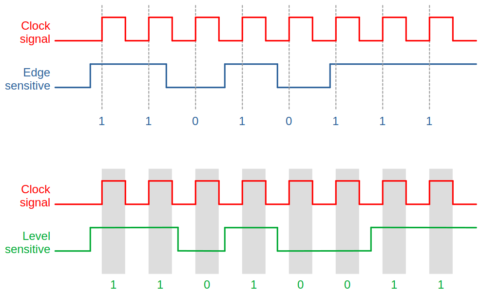
  <li><strong>时钟信号 (clock signal)</strong>：由于数据串行传输，如何控制传输的“时机”就显得尤为重要。一种方法是将一个周期性的信号作为“节拍器”，主机和从机再根据这个“节拍器”来确定何时发数据，何时读数据。这个周期性的信号就被称为时钟信号。需要时钟信号的机制是<strong>同步 (synchronous)</strong> 的，反之就是<strong>异步 (asynchronous)</strong> 的。</li>
  <li><strong>边沿敏感 (edge-sensitive)</strong> 和<strong>电平敏感 (level-sensitive)</strong>：所谓的“边沿”和“电平”以时钟信号为参照。
    <ul>
      <li>边沿是指时钟信号从低电平变为高电平或者由高电平变为低电平的<strong>变化过程</strong>，而“边沿敏感”指的就是数据是在<strong>某个特定的边沿 (上升沿 rising-edge/下降沿 falling-edge) 处被读出</strong>的；</li>
      <li>“电平敏感”指的则是数据是在时钟信号<strong>位于某个特定的电平 (高或低) 时被读出</strong>的。</li>
    </ul>
  </li>
</ul>

<p style="text-align: center;">
  <img src="/assets/images/protocol/edge-level.png" width="500" alt="敏感类型示意图" />
</p>
<p style="text-align: center; color: gray;"><small>边沿敏感 (上升沿) 和电平敏感 (高电平) 的信号示意。</small></p>

<blockquote>
  <p>💡 如果数据信号是边沿敏感的，需要保证其在时钟信号<strong>指定边沿前后的一小段时间内</strong>保持恒定，否则会形成<strong>建立/保持时间违例 (setup/hold time violation)</strong>，容易导致系统进入亚稳态 (metastable state) 并影响功能的正确性。这是由硬件产生的限制，无法根除，且是高频数字 IC 设计的难点。</p>
</blockquote>

<h2 id="spi完整且灵活的通信协议">SPI：完整且灵活的通信协议</h2>

<h3 id="硬件构造">硬件构造</h3>

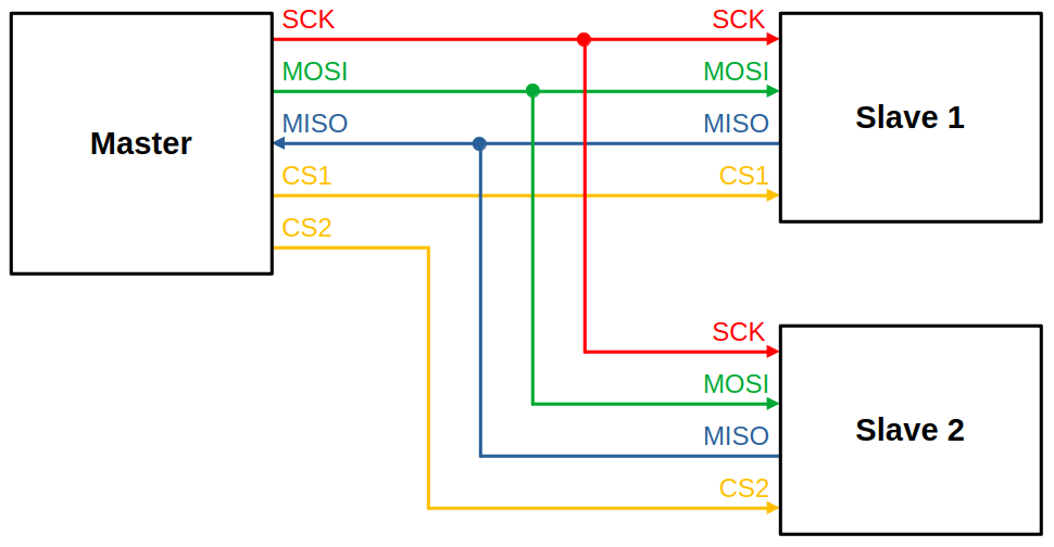
<p>SPI 通信协议支持一个主机与多个从机之间通信，需要四种类型的连线。</p>

<table>
  <thead>
    <tr>
      <th style="text-align: left"><strong>线名</strong></th>
      <th style="text-align: left"><strong>功能</strong></th>
      <th style="text-align: left"><strong>描述</strong></th>
    </tr>
  </thead>
  <tbody>
    <tr>
      <td style="text-align: left"><strong><code class="language-plaintext highlighter-rouge">SCK</code></strong></td>
      <td style="text-align: left">时钟线</td>
      <td style="text-align: left">主机产生；极性和相位可选</td>
    </tr>
    <tr>
      <td style="text-align: left"><strong><code class="language-plaintext highlighter-rouge">CS</code></strong></td>
      <td style="text-align: left">片选线</td>
      <td style="text-align: left">决定主机和哪个从机通信；每个从机一根，低电平有效</td>
    </tr>
    <tr>
      <td style="text-align: left"><strong><code class="language-plaintext highlighter-rouge">MOSI</code></strong></td>
      <td style="text-align: left">主机输出，从机输入</td>
      <td style="text-align: left">传输数据；所有从机共用一根</td>
    </tr>
    <tr>
      <td style="text-align: left"><strong><code class="language-plaintext highlighter-rouge">MISO</code></strong></td>
      <td style="text-align: left">主机输入，从机输出</td>
      <td style="text-align: left">传输数据；所有从机共用一根</td>
    </tr>
  </tbody>
</table>

<p style="text-align: center;">
  <img src="/assets/images/protocol/spi.png" width="500" alt="SPI 协议硬件构造示意图" />
</p>
<p style="text-align: center; color: gray;"><small>SPI 协议硬件构造示意。</small></p>

<p>SPI 协议的设计允许数据以<strong>极高</strong>的速率传输，例如 STM32G473RCT6 就支持最高 8.0 MBit/s 的速率 (每秒传输 800 万个比特位)。同时由于输入和输出线分离，SPI 协议可实现<strong>全双工 (full-duplex)</strong> 通信，即由主机向从机发送的数据和由从机向主机发送的数据能<strong>同时</strong>传输。</p>

<h3 id="数据传输">数据传输</h3>

<h4 id="开始与停止">开始与停止</h4>

<p>SPI 的片选线 <code class="language-plaintext highlighter-rouge">CS</code> 是低电平有效的。因此，SPI 的数据传输由片选线 <code class="language-plaintext highlighter-rouge">CS</code> 被设为低电平开始，在片选线 <code class="language-plaintext highlighter-rouge">CS</code> 被设为高电平时结束。</p>

<h4 id="传输过程">传输过程</h4>

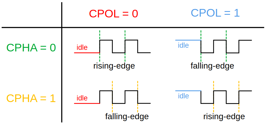
<p>SPI 的数据信号是<strong>边沿敏感</strong>的。其时钟信号由时钟线 <code class="language-plaintext highlighter-rouge">SCK</code> 搭载，我们可以调整<strong>时钟极性 (clock polarity, CPOL)</strong> 和<strong>时钟相位 (clock phase, CPHA)</strong> 来满足不同的外设。</p>

<ul>
  <li>时钟极性 CPOL：时钟<strong>空闲 (idle) 时的电平</strong>，可取 0 或 1：
    <ul>
      <li>0 代表时钟空闲时位于低电平，</li>
      <li>1 代表时钟空闲时位于高电平。</li>
    </ul>
  </li>
  <li>时钟相位 CPHA：数据从时钟信号开始的<strong>第几个边沿开始采样</strong>，可取 0 或 1：
    <ul>
      <li>0 代表使用从时钟信号开始的那个边沿，</li>
      <li>1 代表使用从时钟信号开始的那个边沿的后一个边沿。</li>
    </ul>
  </li>
</ul>

<p style="text-align: center;">
  <img src="/assets/images/protocol/spi-clock.png" width="500" alt="SPI 协议时钟示意图" />
</p>
<p style="text-align: center; color: gray;"><small>SPI 协议时钟极性、时钟相位示意。</small></p>

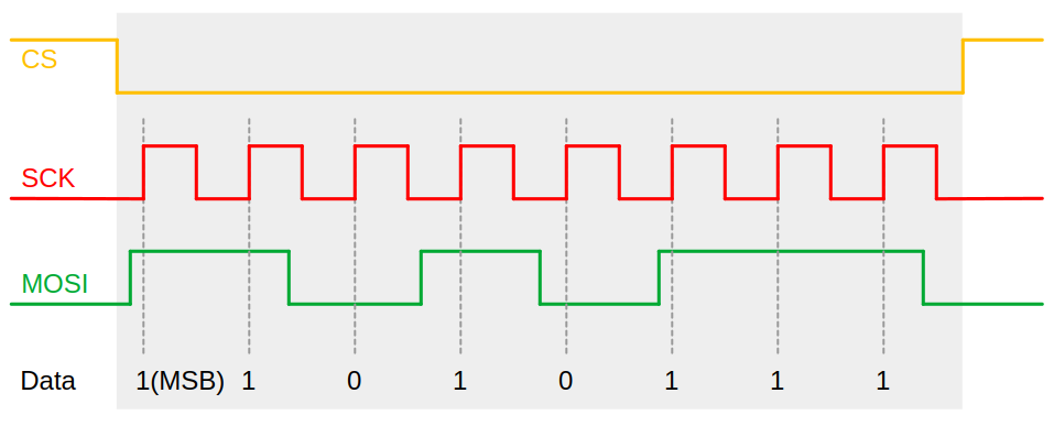
<p>在两根数据线 <code class="language-plaintext highlighter-rouge">MOSI</code> 和 <code class="language-plaintext highlighter-rouge">MISO</code> 上，数据都是<strong>最高位 (MSB) 先出</strong>，意味着数据的高位先传输，低位后传输。下图展示了一个 SPI 协议的传输示例。</p>

<p style="text-align: center;">
  <img src="/assets/images/protocol/spi-transmit.png" width="500" alt="SPI 协议传输示例图" />
</p>
<p style="text-align: center; color: gray;"><small>SPI 协议传输示例：主机向从机发送数据，CPOL = 0，CPHA = 0。</small></p>

<h3 id="具体实现">具体实现</h3>

<p>SPI 传输协议在 MCU 上的实现有软件和硬件两种。</p>

<ul>
  <li>软件 SPI 就是通过 MCU 上的通用输入输出 (GPIO) 端口来控制 SPI 协议的四种连线，再通过<strong>代码操作 GPIO</strong> 来传输数据。</li>
  <li>硬件 SPI 就是借由 MCU <strong>内置的 SPI 相关模块</strong>实现传输，代码层面只需要调用对应的库函数即可。例如，在 STM32G4 系列的 MCU 上配置好相应的引脚后，我们可以直接调用 <code class="language-plaintext highlighter-rouge">HAL_SPI_Transmit</code> 和 <code class="language-plaintext highlighter-rouge">HAL_SPI_Receive</code> 这两个函数来借由 MCU 上的 SPI 模块实现发送与接收数据。</li>
</ul>

<p>软件 SPI 通常比硬件 SPI 的传输速率会低一些。</p>

<blockquote>
  <p>💡 从更广泛的视角来看，解决同一个问题，通常软件实现都会比硬件实现的执行效率低。软件实现是间接的：所有代码最终都要翻译成机器码扔到一个处理器去执行，而处理器为了普适性一般不会为了某个具体的问题作优化。硬件实现则是直接的：将需求一步到位落地实现到数字逻辑中，设计出为了解决这个问题的专用的数字电路，因此可以优化到极致。</p>

  <p>有现实的示例可供参考。在量化交易领域，计算速度至关重要：一个延迟了几毫秒的卖出操作就可能造成几千甚至上万元的损失。除了把计算程序的性能凹到极致，从业人士甚至还开始使用 FPGA (现场可编程门阵列) 来进行相关计算，因为 FPGA 的执行速度更快。FPGA 是更直接的硬件实现，它的内部是一些基本的逻辑元件，可以通过编程把它们连接起来，从而形成某个特定功能的数字电路。</p>
</blockquote>

<p>以下是软件 SPI 的实例，代码基于 STM32G4 系列 MCU。</p>

<div class="language-c highlighter-rouge"><div class="highlight"><pre class="highlight"><code><span class="c1">// CPOL = 0, CPHA = 0</span>
<span class="kt">void</span> <span class="nf">spi_transmit</span><span class="p">(</span><span class="k">const</span> <span class="n">GPIO_TypeDef</span><span class="o">*</span> <span class="n">CS_port</span><span class="p">,</span> <span class="k">const</span> <span class="kt">uint16_t</span> <span class="n">CS_pin</span><span class="p">,</span> <span class="kt">uint8_t</span> <span class="n">data</span><span class="p">)</span> <span class="p">{</span>
  <span class="n">HAL_GPIO_WritePin</span><span class="p">(</span><span class="n">SCK_port</span><span class="p">,</span> <span class="n">SCK_pin</span><span class="p">,</span> <span class="n">GPIO_PIN_RESET</span><span class="p">);</span> <span class="c1">// SCK low, idle </span>
  <span class="n">HAL_GPIO_WritePin</span><span class="p">(</span><span class="n">CS_port</span><span class="p">,</span> <span class="n">CS_pin</span><span class="p">,</span> <span class="n">GPIO_PIN_RESET</span><span class="p">);</span> <span class="c1">// CS low, start transmission</span>

  <span class="k">for</span> <span class="p">(</span><span class="kt">int</span> <span class="n">i</span> <span class="o">=</span> <span class="mi">7</span><span class="p">;</span> <span class="n">i</span> <span class="o">&gt;=</span> <span class="mi">0</span><span class="p">;</span> <span class="o">--</span><span class="n">i</span><span class="p">)</span> <span class="p">{</span> <span class="c1">// MSB first</span>
    <span class="n">HAL_GPIO_WritePin</span><span class="p">(</span><span class="n">MOSI_port</span><span class="p">,</span> <span class="n">MOSI_pin</span><span class="p">,</span> <span class="p">(</span><span class="n">data</span> <span class="o">&amp;</span> <span class="p">(</span><span class="mi">1</span> <span class="o">&lt;&lt;</span> <span class="n">i</span><span class="p">))</span> <span class="o">?</span> <span class="n">GPIO_PIN_SET</span> <span class="o">:</span> <span class="n">GPIO_PIN_RESET</span><span class="p">);</span>
    <span class="n">HAL_GPIO_WritePin</span><span class="p">(</span><span class="n">SCK_port</span><span class="p">,</span> <span class="n">SCK_pin</span><span class="p">,</span> <span class="n">GPIO_PIN_SET</span><span class="p">);</span> <span class="c1">// SCK high, rising edge</span>
    <span class="n">HAL_GPIO_WritePin</span><span class="p">(</span><span class="n">SCK_port</span><span class="p">,</span> <span class="n">SCK_pin</span><span class="p">,</span> <span class="n">GPIO_PIN_RESET</span><span class="p">);</span> <span class="c1">// SCK back to low</span>
  <span class="p">}</span>

  <span class="n">HAL_GPIO_WritePin</span><span class="p">(</span><span class="n">CS_port</span><span class="p">,</span> <span class="n">CS_pin</span><span class="p">,</span> <span class="n">GPIO_PIN_SET</span><span class="p">);</span> <span class="c1">// CS high, end transmission</span>
  <span class="n">HAL_GPIO_WritePin</span><span class="p">(</span><span class="n">SCK_port</span><span class="p">,</span> <span class="n">SCK_pin</span><span class="p">,</span> <span class="n">GPIO_PIN_RESET</span><span class="p">);</span> <span class="c1">// SCK low, back to idle </span>
<span class="p">}</span>
</code></pre></div></div>

<h2 id="i2c一根数据线控制权的巧妙调度">I2C：一根数据线控制权的巧妙调度</h2>

<p>我们可以发现，SPI 有一个缺点：连线的数量还是太多了，尤其是片选线，每个从机都需要有一根。有没有办法减少连线的数量呢？</p>

<p>有的兄弟，有的。请看 I2C。</p>

<h3 id="硬件构造-1">硬件构造</h3>

<p>I2C 通信协议支持多个主机和多个从机之间的通信。它只需要两根线。</p>

<table>
  <thead>
    <tr>
      <th style="text-align: left"><strong>线名</strong></th>
      <th style="text-align: left"><strong>功能</strong></th>
      <th style="text-align: left"><strong>描述</strong></th>
    </tr>
  </thead>
  <tbody>
    <tr>
      <td style="text-align: left"><strong><code class="language-plaintext highlighter-rouge">SCL</code></strong></td>
      <td style="text-align: left">时钟线</td>
      <td style="text-align: left">主机产生，从机可以根据自身处理情况延长低电平时间</td>
    </tr>
    <tr>
      <td style="text-align: left"><strong><code class="language-plaintext highlighter-rouge">SDA</code></strong></td>
      <td style="text-align: left">数据线</td>
      <td style="text-align: left">用于主机和从机之间双向传输数据</td>
    </tr>
  </tbody>
</table>

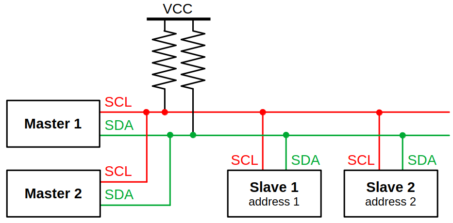
<p>由于没有片选线，I2C 要求系统里的每个从机都要有一个独一无二的<strong>地址 (address)</strong> 以方便主机区分。</p>

<p style="text-align: center;">
  <img src="/assets/images/protocol/i2c.png" width="500" alt="I2C 协议硬件构造示意图" />
</p>
<p style="text-align: center; color: gray;"><small>I2C 协议硬件线路连接示意。</small></p>

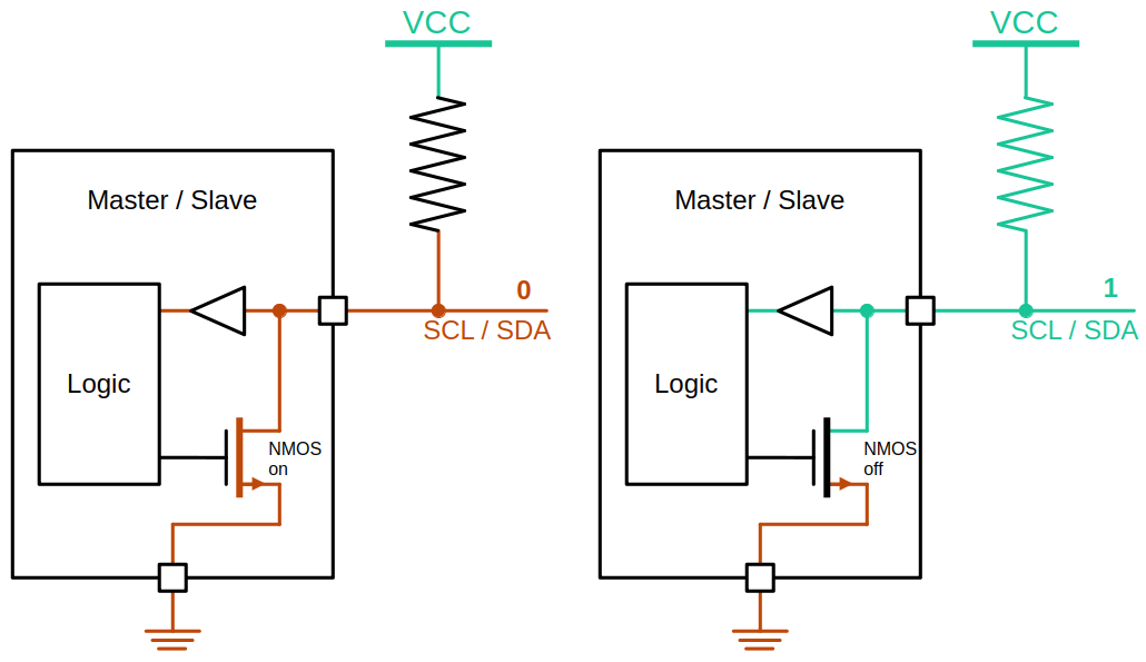
<p>我们看到，I2C 协议的时钟线 <code class="language-plaintext highlighter-rouge">SCL</code> 和数据线 <code class="language-plaintext highlighter-rouge">SDA</code> 都连接了一个上拉电阻 (pull-up resistor)。而在每个设备内，两根线各自都通过一个 NMOS 三极管接地。这与 I2C 产生电平的机制有关：</p>

<ul>
  <li>某个设备想输出低电平时，就<strong>让其 NMOS 三极管导通，将对应的线接地</strong>；</li>
  <li>某个设备想输出高电平时，就<strong>断开其 NMOS 三极管释放对应的线，上拉电阻会把它拉到高电平</strong>。</li>
</ul>

<p>因此，当空闲时，两根线都会处于高电平。</p>

<p style="text-align: center;">
  <img src="/assets/images/protocol/i2c-pullup.png" width="500" alt="I2C 协议电平产生示意图" />
</p>
<p style="text-align: center; color: gray;"><small>I2C 协议产生电平的机制。</small></p>

<blockquote>
  <p>💡 NMOS 三极管是 MOSFET (金属氧化物半导体场效应晶体管) 中的一种。NMOS 有三个端口，图中右上、右下的端口分别是漏极 (drain) 和源极 (source)，左侧的端口是栅极 (gate)。在这个电路中，NMOS 可以看作是一个由栅极电平控制的开关：当栅极为低电平的时候，源极和漏极之间不导通，开关断开；当栅极为高电平的时候，源极和漏极之间导通，开关闭合。</p>
</blockquote>

<p>这种连接还产生了一个<strong>线与门 (wired-AND)</strong> 的效应：当多个设备想要往同一根线上输出的时候，</p>

<ul>
  <li>只有这些设备都想要输出高电平的时候，这根线才会是高电平；</li>
  <li>反之，只要有一个设备想输出低电平的时候，这根线就是低电平。</li>
</ul>

<p>I2C 利用这一效应避免了短路 (<code class="language-plaintext highlighter-rouge">VCC</code> 直接接地)，还实现了很多巧妙的机制，我们一会儿会讲到。</p>

<hr />

<p>然而，由于 I2C 的高电平不是硬连接到 <code class="language-plaintext highlighter-rouge">VCC</code> 而是靠上拉电阻实现，电源就需要通过上拉电阻给整条线路的寄生电容 (parasitic capacitance) 充电。而上拉电阻的阻值一般不会太小，所以这个 RC 电路的时间常数比较大，因而<strong>从低电平到高电平的转换就会较为缓慢</strong>。这限制了 I2C 的传输速率，使其无法达到 SPI 的水平 (例如 STM32G473RCT6 的 I2C 最高传输速率只有 400 kBit/s，即每秒传输 40 万个比特位)。</p>

<p>此外，由于只有一根数据线，虽然主机可以向从机发送数据，从机也可以向主机发送数据，但是这两者<strong>不能同时进行</strong>。因此，I2C 只能实现<strong>半双工 (half-duplex)</strong>。</p>

<h3 id="数据传输-1">数据传输</h3>

<h4 id="开始与停止-1">开始与停止</h4>

<p>I2C 的开始和停止比较特殊：</p>

<ul>
  <li><strong>开始条件 (START condition)</strong>：在 <code class="language-plaintext highlighter-rouge">SCL</code> 为高电平时，<code class="language-plaintext highlighter-rouge">SDA</code> 由高电平变为低电平；</li>
  <li><strong>停止条件 (STOP condition)</strong>：在 <code class="language-plaintext highlighter-rouge">SCL</code> 为高电平时，<code class="language-plaintext highlighter-rouge">SDA</code> 由低电平变为高电平。</li>
</ul>

<p>除此之外，还存在一个重复开始条件 (repeated START condition)，是在主机希望发起一个新的通信请求，但是不想发送停止条件从而释放两根线的控制权时使用的。</p>

<h4 id="传输过程-1">传输过程</h4>

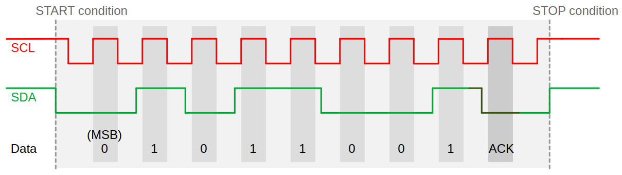
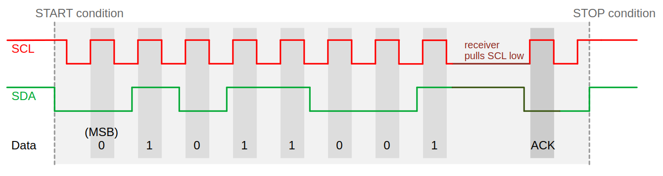
<p>I2C 的数据信号是<strong>电平敏感</strong>的。除了开始和停止条件之外，数据线 <code class="language-plaintext highlighter-rouge">SDA</code> 上的所有电平都是在时钟线 <code class="language-plaintext highlighter-rouge">SCL</code> 位于<strong>高电平时读取</strong>的。因此，在每个 <code class="language-plaintext highlighter-rouge">SCL</code> 的高电平期间，<code class="language-plaintext highlighter-rouge">SDA</code> 的电平应保持稳定，否则会被认为是开始或停止条件，导致执行错误。</p>

<p>在数据线 <code class="language-plaintext highlighter-rouge">SDA</code> 上，数据都是<strong>最高位先出</strong>的，且一般以<strong>字节为单位</strong>。I2C 还引入了确认 (acknowledge, ACK) 和不确认 (not acknowledge, NACK) 机制来让发送者知晓数据的接收情况：在每个字节发送完毕后，发送者会暂时释放数据线 <code class="language-plaintext highlighter-rouge">SDA</code> 一个时钟周期，接收者在这个时钟周期内会控制 <code class="language-plaintext highlighter-rouge">SDA</code> 的电平：</p>

<ul>
  <li>高电平表示不确认 (NACK)，接收者无法或不愿再接收数据；</li>
  <li>低电平表示确认 (ACK)，接收者完整收到并处理了数据，告知发送者可进行接下来的操作。</li>
</ul>

<p>需要注意的是，发送者不一定是主机，接收者也不一定是从机。从机也可以向主机发送数据。</p>

<blockquote>
  <p>💡 ACK 与 NACK 的电平高低是有讲究的：在一切正常的时候，接收者需要对数据线 <code class="language-plaintext highlighter-rouge">SDA</code> 的电平进行主动的操作。如果接收者本身故障了完全没有反应，它就不会动 <code class="language-plaintext highlighter-rouge">SDA</code> 的电平；而 <code class="language-plaintext highlighter-rouge">SDA</code> 的电平空闲时是高，对应 NACK，发送者一看，就知晓自己发送的数据并没有被接收者接收到。</p>
</blockquote>

<p style="text-align: center;">
  <img src="/assets/images/protocol/i2c-transmit.png" width="500" alt="I2C 协议字节传输示意图" />
</p>
<p style="text-align: center; color: gray;"><small>I2C 协议传输一个字节的过程示意 (接收者在最后发送 ACK)。</small></p>

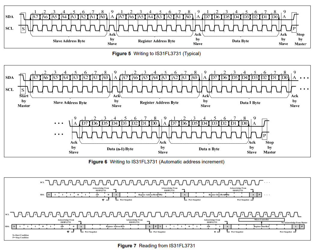
<p>I2C 的数据传输往往还遵循固定的格式。不同从机可能对数据的格式有不同的要求，但是大多数都包含<strong>从机地址</strong>、<strong>从机内部的寄存器地址</strong>，还有要传输的<strong>数据本体</strong>。以下图片来源于 IS31FL3731 的手册，它是一个 LED 矩阵的驱动器，使用 I2C 与 MCU 之间进行通信。</p>

<p style="text-align: center;">
  <img src="/assets/images/protocol/i2c-format.png" width="600" alt="I2C 协议传输格式示例图" />
</p>
<p style="text-align: center; color: gray;"><small>IS31FL3731 规定的数据传输格式。图片取自 IS31FL3731 的手册。</small></p>

<h3 id="特殊机制">特殊机制</h3>

<p>当一个多主机的系统采用 I2C 协议进行通信的时候，如何有序、高效地调度线路的控制权，就成为了一个问题。这时，I2C 协议的“线与门”机制就可以发挥威力了。</p>

<h4 id="时钟同步-clock-synchronization">时钟同步 (Clock Synchronization)</h4>

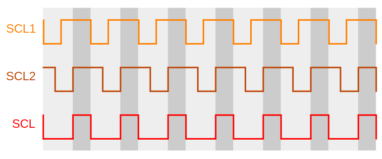
<p>多个主机产生的时钟信号虽然可以设置为相同的频率，但是相位和占空比很难保证完全一致。如何确定一个稳定的时钟信号，保证数据线 <code class="language-plaintext highlighter-rouge">SDA</code> 在这个时钟信号为高电平时是恒定的呢？</p>

<p>我们想到，在所有主机各自产生的时钟信号均为高电平时，它们<em>想要</em>往数据线 <code class="language-plaintext highlighter-rouge">SDA</code> 上输出的数据都是恒定的，所以 <code class="language-plaintext highlighter-rouge">SDA</code> 的电平就<strong>一定是恒定的</strong>。因此，这个稳定的时钟信号就可以通过所有的时钟信号<strong>取与</strong>获得。这并不需要任何额外的器件，因为 <code class="language-plaintext highlighter-rouge">SCL</code> 天然具有线与门的特性！这就是<strong>时钟同步</strong>。</p>

<p style="text-align: center;">
  <img src="/assets/images/protocol/i2c-clock.png" width="500" alt="I2C 时钟同步示意图" />
</p>
<p style="text-align: center; color: gray;"><small>I2C 的时钟同步机制示意。</small></p>

<h4 id="仲裁-arbitration">仲裁 (Arbitration)</h4>

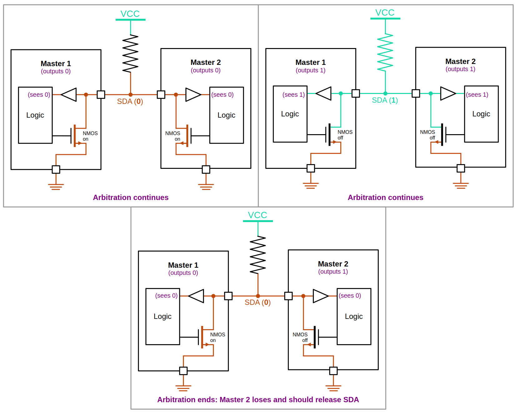
<p>时钟是同步了，但是多个主机会尝试在同一个时间点开始发送数据，产生控制权的争夺。I2C 通过<strong>仲裁</strong>来确定哪个主机获得最终的控制权。</p>

<p>仲裁的规则十分简单：我们没办法阻止主机在同一个时间点开始发送数据，那就让它们一边发送各自的数据一边盯着数据线 <code class="language-plaintext highlighter-rouge">SDA</code> 看，<strong>谁先往 <code class="language-plaintext highlighter-rouge">SDA</code> 上发送高电平但是看到低电平，谁输掉仲裁 (lose arbitration) 并退出。</strong>输掉仲裁的主机需要释放 <code class="language-plaintext highlighter-rouge">SDA</code>，等待观测到停止条件后才能重新尝试发送数据。这一仲裁机制是<strong>去中心化</strong>的，没有一个统一的上层单元指挥，全靠各个主机的“自觉”判定。</p>

<p>由于 <code class="language-plaintext highlighter-rouge">SDA</code> 的线与门特性，某个主机因输掉仲裁而退出时，不会对仍在场上发送数据的主机产生任何影响，因为它尝试发送的是高电平；而输掉仲裁前，它们发送的一定是相同的数据。因此仲裁的过程对于所有从机而言都是<strong>透明</strong>的，无法察觉。</p>

<p style="text-align: center;">
  <img src="/assets/images/protocol/i2c-arbitration.png" width="700" alt="I2C 仲裁示意图" />
</p>
<p style="text-align: center; color: gray;"><small>I2C 的仲裁机制示意。</small></p>

<h4 id="时钟拉伸-clock-stretching">时钟拉伸 (Clock Stretching)</h4>

<p>有时，从机处理主机发送来的数据需要一定时间。由于时钟信号的产生并不由从机控制，如果在处理完成前主机发送的新数据就到达了，或者从机忙于处理数据没能及时拉低数据线 <code class="language-plaintext highlighter-rouge">SDA</code> 来应答 ACK，很容易造成传输的混乱和效率低下。</p>

<p>但是从机也并非束手无策。从机可以通过<strong>主动拉低时钟线 <code class="language-plaintext highlighter-rouge">SCL</code> 来延伸某个时钟周期低电平的时间</strong>，从而完成数据的处理。由于 <code class="language-plaintext highlighter-rouge">SCL</code> 具有线与门的特性，只要从机将其拉低，即使主机产生的时钟信号想将其置高，它也仍然是低电平。主机在观测这种情况时，也需要相应地延长自己产生的时钟信号的低电平时间，直至从机完成数据处理释放 <code class="language-plaintext highlighter-rouge">SCL</code>。这就是<strong>时钟拉伸</strong>。</p>

<p style="text-align: center;">
  <img src="/assets/images/protocol/i2c-extension.png" width="550" alt="I2C 时钟拉伸示意图" />
</p>
<p style="text-align: center; color: gray;"><small>I2C 的时钟拉伸机制示意。</small></p>

<h3 id="具体实现-1">具体实现</h3>

<p>I2C 协议在 MCU 上的实现也有两种，硬件 I2C 和软件 I2C。但是由于 I2C 的机制比较复杂，软件实现也会很繁琐且执行效率低下，因此绝大部分情境下 I2C 协议都是通过硬件来实现的。在 STM32G4 系列 MCU 上，配置好 I2C 模块对应的引脚之后，代码中可以直接调用 <code class="language-plaintext highlighter-rouge">HAL_I2C_Master_Transmit</code> 和 <code class="language-plaintext highlighter-rouge">HAL_I2C_Master_Receive</code> 函数来实现硬件 I2C 向从机传输和接受数据。</p>

<h2 id="uart去除时钟线实现异步全双工">UART：去除时钟线，实现异步全双工</h2>

<p>I2C 协议的线路数量虽然只有 2 根，但是它只有一根数据线 <code class="language-plaintext highlighter-rouge">SDA</code>，只能实现半双工，就像单线铁路：如果有两列不同方向的列车交汇，其中一列就需要停车等待另一列完全通过之后才能通过。有没有办法既保留 I2C 线路少的优势，同时又将其改造成“双线铁路”实现全双工呢？</p>

<p>我们自然而然地把目光投向 I2C 的另一根时钟线 <code class="language-plaintext highlighter-rouge">SCL</code>，它的存在意味着 I2C 协议是同步的。如果把它砍了换成另一根数据线，就能重新实现全双工，但传输变成了<strong>异步</strong>。这就是 UART。</p>

<h3 id="硬件构造-2">硬件构造</h3>

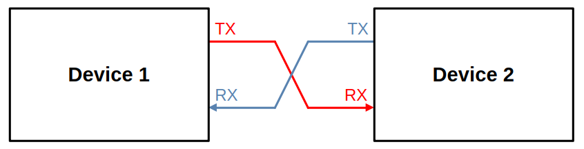
<p>UART 协议只支持两个设备之间的通信，且没有严格的主机从机之分，因为两台设备的构造完全一致。每个设备均有两个端口，</p>

<ul>
  <li><strong><code class="language-plaintext highlighter-rouge">RX</code></strong> 用来接收数据，</li>
  <li><strong><code class="language-plaintext highlighter-rouge">TX</code></strong> 用来发送数据。</li>
</ul>

<p>每台设备的 <code class="language-plaintext highlighter-rouge">RX</code> 端口都与另一台设备的 <code class="language-plaintext highlighter-rouge">TX</code> 端口相连。这就实现了<strong>全双工</strong>，两台设备之间可以同时互相传输数据。</p>

<p style="text-align: center;">
  <img src="/assets/images/protocol/uart.png" width="500" alt="UART 协议硬件构造示意图" />
</p>
<p style="text-align: center; color: gray;"><small>UART 协议硬件线路连接示意。</small></p>

<blockquote>
  <p>💡 一般来说，UART 应用在电脑主机与 MCU 之间的通信。在这种情况下，电脑主机通常被称为<strong>上位机 (host computer)</strong>。</p>
</blockquote>

<h3 id="数据传输-2">数据传输</h3>

<h4 id="开始与停止-2">开始与停止</h4>

<p><code class="language-plaintext highlighter-rouge">RX</code>/<code class="language-plaintext highlighter-rouge">TX</code> 在空闲时为高电平。当 <code class="language-plaintext highlighter-rouge">RX</code>/<code class="language-plaintext highlighter-rouge">TX</code> 由高电平变为低电平时，传输开始；当数据传输完毕后，<code class="language-plaintext highlighter-rouge">RX</code>/<code class="language-plaintext highlighter-rouge">TX</code> 由低电平变为高电平，传输停止。开始和停止的条件在发生后也占一个数据位的时间，称为起始位 (START bit) 和停止位 (STOP bit)。</p>

<h4 id="传输过程-2">传输过程</h4>

<p>由于没有统一的时钟来指挥，两台设备必须提前约定好很多东西，其中就包括<strong>波特率 (baud rate)</strong>。波特率是指每秒传输的符号数，单位 baud。在 UART 的语境下，<strong>波特率就等于每秒传输的比特位的数量</strong>，因为一个比特就由信号中的一个符号携带。UART 协议常用的波特率有 9600、19200 和 115200。</p>

<p>虽然波特率设为一致了，但是接收方看到的仍然只是一个光秃秃的数据信号。如果它一个周期只对这个数据信号采样一次，很容易出现严重的错误，因为<strong>没有参照点</strong>。UART 协议解决这个问题的方法是<strong>起始位同步 (START bit synchronization)</strong> 和<strong>过采样 (oversampling)</strong>：接收方在观测到起始位之后才开始接收数据，同时需要以约定好的波特率的若干倍来对数据信号采样。这个倍数一般是 2 的幂，通常采用 8、16 或者 32。</p>

<p>以 16 倍过采样为例，每 16 个采样周期对应一个数据位。接收者的采样流程如下：</p>

<ul>
  <li>观测到 <code class="language-plaintext highlighter-rouge">RX</code> 由高变低，开始采样；</li>
  <li>经过 8 个采样周期后，观察 <code class="language-plaintext highlighter-rouge">RX</code> 是否仍为低，若是，将其作为起始位的中心点；若不是，则之前观测到的 <code class="language-plaintext highlighter-rouge">RX</code> 由高变低是噪声毛刺，停止采样。</li>
  <li>每隔 16 个采样周期对 <code class="language-plaintext highlighter-rouge">RX</code> 进行采样，作为一个新的数据位的中心点；</li>
  <li>在接收数据完毕之后停止采样。</li>
</ul>

<p>此外，两台设备还需规定起始位和停止位之间传输多少比特位，在整个通信过程中都需要保持一致。我们还可以选择在一个数据传输完毕后添加一个<strong>奇偶校验位 (parity bit)</strong>，表示传输的数据中应该有奇数个还是偶数个高电平，方便接收者检验。</p>

<p style="text-align: center;">
  <img src="/assets/images/protocol/uart-transmit.png" width="550" alt="UART 协议数据传输示意图" />
</p>
<p style="text-align: center; color: gray;"><small>UART 协议硬数据传输示意：16 倍过采样，3 个数据位，无校验位。</small></p>

<hr />

<p>当然，就像对好的时钟经过一段时间后会不精确一样，两台设备各自的波特率也可能会有小幅的差异，引起误差累积。不过理论上这个误差的影响不是很大，因为</p>

<ul>
  <li>每次数据传输之前都有起始位同步，因而误差累积被限制在一次数据传输之内；</li>
  <li>通过过采样并且选择合适的采样时间点，我们还保证每次采样都大致在数据信号的中心点，即使有小幅误差也很难读取到错误的电平。</li>
</ul>

<p>实际应用中，UART 协议可以忍受<strong>两台设备之间的波特率误差在 4%</strong> 左右。</p>

<h3 id="具体实现-2">具体实现</h3>

<p>UART 协议一般通过专门的硬件实现，代码中只需要调用对应的底层函数即可。</p>

<p>除提供的底层函数之外，还存在许多开源的 UART 库可供使用，能极大简便调试和开发。例如，<a href="https://github.com/jerry-fuyi/SerialAccessor">SerialAccessor</a> 就是一个通过 UART 实现上位机对 MCU 寄存器直接访问的串口调试框架。有时间的话，我也会详细解析一下这个框架的运行机制，包括 DMA 缓冲区等等。</p>

<h2 id="总结">总结</h2>

<p>我们详细讲述了 SPI、I2C，以及 UART 串口通信协议的基本原理。在实际应用中，可根据它们的特点和实际需求灵活使用。</p>

<table>
  <thead>
    <tr>
      <th style="text-align: left"><strong>协议</strong></th>
      <th style="text-align: left"><strong>时序类型</strong></th>
      <th style="text-align: left"><strong>传输模式</strong></th>
      <th style="text-align: left"><strong>主从机数量</strong></th>
      <th style="text-align: left"><strong>端口数量</strong></th>
      <th style="text-align: left"><strong>从机选择方式</strong></th>
      <th style="text-align: left"><strong>传输速率</strong></th>
    </tr>
  </thead>
  <tbody>
    <tr>
      <td style="text-align: left"><strong>SPI</strong></td>
      <td style="text-align: left">同步</td>
      <td style="text-align: left">全双工</td>
      <td style="text-align: left">一主多从</td>
      <td style="text-align: left">至少 3</td>
      <td style="text-align: left">片选线 <code class="language-plaintext highlighter-rouge">CS</code></td>
      <td style="text-align: left">很高</td>
    </tr>
    <tr>
      <td style="text-align: left"><strong>I2C</strong></td>
      <td style="text-align: left">同步</td>
      <td style="text-align: left">半双工</td>
      <td style="text-align: left">多主多从</td>
      <td style="text-align: left">2</td>
      <td style="text-align: left">从机地址</td>
      <td style="text-align: left">较低</td>
    </tr>
    <tr>
      <td style="text-align: left"><strong>UART</strong></td>
      <td style="text-align: left">异步</td>
      <td style="text-align: left">全双工</td>
      <td style="text-align: left">一对一</td>
      <td style="text-align: left">2</td>
      <td style="text-align: left">-</td>
      <td style="text-align: left">较低</td>
    </tr>
  </tbody>
</table>

<h2 id="参考资料">参考资料</h2>

<ul>
  <li><a href="https://www.ti.com/lit/ab/sboa621/sboa621.pdf">Understanding the SPI Bus (SBOA621)</a> - Texas Instruments</li>
  <li><a href="https://www.ti.com/lit/an/slva704/slva704.pdf">Understanding the I2C Bus (SLVA704)</a> - Texas Instruments</li>
  <li><a href="https://www.ti.com/content/dam/videos/external-videos/en-us/8/3816841626001/6243124608001.mp4/subassets/adcs-introduction-to-i2c-advanced-topics-presentation.pdf">Basics of I2C: Advanced Topics (TIPL6104)</a> - Texas Instruments</li>
  <li><a href="https://www.ti.com/content/dam/videos/external-videos/en-us/9/3816841626001/6313217959112.mp4/subassets/uart_protocol_overview_and_error_sources_0.pdf">UART Protocol Overview</a> - Texas Instruments</li>
  <li><a href="https://lumissil.com/assets/pdf/core/IS31FL3731_DS.pdf">IS31FL3731: Audio Modulated Matrix LED Driver</a> - Lumissil Microsystems</li>
  <li><a href="https://www.st.com/resource/en/user_manual/um2570-description-of-stm32g4-hal-and-lowlayer-drivers--stmicroelectronics.pdf">Description of STM32G4 HAL and low-layer drivers (UM2570)</a> - ST Microelectronics</li>
</ul>]]></content><author><name></name></author><category term="zh-cn" /><category term="embedded" /><category term="communication" /><summary type="html"><![CDATA[在进行嵌入式开发时，我们常常需要让 MCU (microcontroller unit，即俗称的“单片机”) 与外围设备 (peripheral，外设) 交换信息，包括 LED 矩阵、LCD 显示屏等等。在人类社会中，信息的交换绝大部分是通过语言文字实现的；而在嵌入式领域，MCU 与外设之间的信息交换也有自己的“语言”，我们通常称之为通信协议 (communication protocol)。]]></summary></entry><entry><title type="html">SPI, I2C, UART: An Introduction to Serial Communication Protocols</title><link href="https://tomategg-101325.github.io/en-us/2026/06/13/spi-i2c-uart-en.html" rel="alternate" type="text/html" title="SPI, I2C, UART: An Introduction to Serial Communication Protocols" /><published>2026-06-13T02:00:00+00:00</published><updated>2026-06-13T02:00:00+00:00</updated><id>https://tomategg-101325.github.io/en-us/2026/06/13/spi-i2c-uart-en</id><content type="html" xml:base="https://tomategg-101325.github.io/en-us/2026/06/13/spi-i2c-uart-en.html"><![CDATA[<p>In embedded development, we often need to let an MCU (microcontroller unit) exchange information with peripherals, such as LED matrices, LCD displays, and so on. In the human society, information exchange is mostly achieved through language, either spoken or written; in the embedded realm, information exchange between an MCU and peripherals also has its own <em>language</em>, which we usually call a <strong>communication protocol</strong>.</p>

<p>The fastest form of information exchange is <strong>parallel</strong>, where all the bits of a piece of data are transmitted simultaneously over many wires—like building a multi-lane highway where many cars can travel at the same time. However, in embedded design, hardware resources are often very limited, and pulling a dozen wires from a device solely to transmit a specific type of data is highly impractical. In this case, <strong>serial</strong> communication becomes essential: it transmits the bits of the data one after another in the time domain over just two or three wires, like opening a narrow country lane where cars must pass one by one.</p>

<p>Although serial transmission is often several times slower than parallel, it greatly reduces the required area and number of pins, making it much more economical. Moreover, today’s hardware can usually process data at megahertz frequencies; the extra time needed rarely has a significant impact in most real-world scenarios.</p>

<p>The three most commonly used serial communication protocols are:</p>

<ul>
  <li><strong>SPI</strong>: Serial Peripheral Interface;</li>
  <li><strong>I2C</strong>: Inter-Integrated Circuit;</li>
  <li><strong>UART</strong>: Universal Asynchronous Receiver/Transmitter.</li>
</ul>

<p>This article covers the hardware configuration, data transmission, and special mechanisms of these three protocols.</p>

<p>Note: This post is a translated version. See <a href="/zh-cn/2026/06/13/spi-i2c-uart-cn.html">here</a> for the original content.</p>

<h2 id="fundamental-concepts">Fundamental Concepts</h2>

<p>Before diving into the details of the protocols, let’s look at a few fundamental concepts involved in transmission.</p>

<ul>
  <li><strong>Master</strong> and <strong>Slave</strong>: The device that <strong>initiates</strong> the communication is called the master; the other devices are called slaves. In most cases, the MCU acts as the master and the peripheral as the slave. Note that a slave can also send data to the master; who is the master and who is the slave is determined by which device initiates the entire transfer.</li>
  <li><strong>Clock Signal</strong>: Since data is transmitted serially, controlling the “timing” of transmission becomes particularly important. One approach is to use a periodic signal as a <em>metronome</em>, with the master and slave then using this metronome to determine when to send data and when to read it. This periodic signal is called the clock signal. Protocols that require a clock signal are <strong>synchronous</strong>; those that do not are <strong>asynchronous</strong>.</li>
  <li><strong>Edge-sensitive</strong> and <strong>Level-sensitive</strong>: The terms “edge” and “level” refer to the clock signal.
    <ul>
      <li>An edge is the <strong>transition process</strong> of the clock signal from low to high or from high to low. “Edge-sensitive” means data is read <strong>at a specific edge (rising edge or falling edge)</strong>.</li>
      <li>“Level-sensitive” means data is read while the clock signal is <strong>at a specific level (high or low)</strong>.</li>
    </ul>
  </li>
</ul>

<p style="text-align: center;">
  <img src="/assets/images/protocol/edge-level.png" width="500" alt="Edge-sensitive and level-sensitive signal illustration" />
</p>
<p style="text-align: center; color: gray;"><small>Edge-sensitive (rising edge) and level-sensitive (high level) signal illustration.</small></p>

<blockquote>
  <p>💡 If a data signal is edge-sensitive, it must remain stable for a short period <strong>before and after the specified clock edge</strong>; otherwise, a <strong>setup/hold time violation</strong> may occur, easily driving the system into a metastable state and affecting functional correctness. This is a hardware limitation that cannot be eliminated and is a challenge in high-frequency digital IC design.</p>
</blockquote>

<h2 id="spi-a-complete-and-flexible-communication-protocol">SPI: A Complete and Flexible Communication Protocol</h2>

<h3 id="hardware-configuration">Hardware Configuration</h3>

<p>The SPI protocol supports communication between one master and multiple slaves and requires four types of connections.</p>

<table>
  <thead>
    <tr>
      <th style="text-align: left"><strong>Wire Name</strong></th>
      <th style="text-align: left"><strong>Function</strong></th>
      <th style="text-align: left"><strong>Description</strong></th>
    </tr>
  </thead>
  <tbody>
    <tr>
      <td style="text-align: left"><strong><code class="language-plaintext highlighter-rouge">SCK</code></strong></td>
      <td style="text-align: left">Clock wire</td>
      <td style="text-align: left">Generated by the master; polarity and phase selectable</td>
    </tr>
    <tr>
      <td style="text-align: left"><strong><code class="language-plaintext highlighter-rouge">CS</code></strong></td>
      <td style="text-align: left">Chip Select wire</td>
      <td style="text-align: left">Determines which slave the master talks to; one per slave, active low</td>
    </tr>
    <tr>
      <td style="text-align: left"><strong><code class="language-plaintext highlighter-rouge">MOSI</code></strong></td>
      <td style="text-align: left">Master Out Slave In</td>
      <td style="text-align: left">Data wire; shared by all slaves</td>
    </tr>
    <tr>
      <td style="text-align: left"><strong><code class="language-plaintext highlighter-rouge">MISO</code></strong></td>
      <td style="text-align: left">Master In Slave Out</td>
      <td style="text-align: left">Data wire; shared by all slaves</td>
    </tr>
  </tbody>
</table>

<p style="text-align: center;">
  <img src="/assets/images/protocol/spi.png" width="500" alt="SPI protocol hardware configuration diagram" />
</p>
<p style="text-align: center; color: gray;"><small>SPI protocol hardware configuration.</small></p>

<p>The SPI design allows data to be transmitted at <strong>extremely</strong> high speeds; for example, the STM32G473RCT6 supports a rate of up to 8.0 MBit/s (8 million bits per second). Moreover, because the input and output wires are separate, SPI can achieve <strong>full-duplex</strong> communication—data sent from the master to the slave and from the slave to the master can be transmitted <strong>simultaneously</strong>.</p>

<h3 id="data-transmission">Data Transmission</h3>

<h4 id="start-and-stop">Start and Stop</h4>

<p>The SPI chip select wire <code class="language-plaintext highlighter-rouge">CS</code> is active low. Therefore, data transmission begins when <code class="language-plaintext highlighter-rouge">CS</code> is set low and ends when <code class="language-plaintext highlighter-rouge">CS</code> is set high.</p>

<h4 id="transmission-process">Transmission Process</h4>

<p>SPI data signals are <strong>edge-sensitive</strong>. The clock signal is carried on the <code class="language-plaintext highlighter-rouge">SCK</code> wire, and we can adjust the <strong>clock polarity (CPOL)</strong> and <strong>clock phase (CPHA)</strong> to meet the requirements of different peripherals.</p>

<ul>
  <li>Clock Polarity (CPOL): The <strong>idle state level</strong> of the clock. It can be 0 or 1:
    <ul>
      <li>0 means the clock idles low,</li>
      <li>1 means the clock idles high.</li>
    </ul>
  </li>
  <li>Clock Phase (CPHA): Which edge of the clock signal to use for sampling, counted <strong>from the start of the clock signal</strong>. It can be 0 or 1:
    <ul>
      <li>0 means use the first edge after the clock signal starts,</li>
      <li>1 means use the second edge after the clock signal starts.</li>
    </ul>
  </li>
</ul>

<p style="text-align: center;">
  <img src="/assets/images/protocol/spi-clock.png" width="500" alt="SPI clock polarity and clock phase illustration" />
</p>
<p style="text-align: center; color: gray;"><small>SPI clock polarity and clock phase illustration.</small></p>

<p>On both the <code class="language-plaintext highlighter-rouge">MOSI</code> and <code class="language-plaintext highlighter-rouge">MISO</code> data wires, data is sent <strong>most significant bit (MSB) first</strong>, meaning the higher bits are transmitted before the lower bits. The figure below shows an example of an SPI transmission.</p>

<p style="text-align: center;">
  <img src="/assets/images/protocol/spi-transmit.png" width="500" alt="SPI transmission example" />
</p>
<p style="text-align: center; color: gray;"><small>SPI transmission example: master sends data to slave, CPOL = 0, CPHA = 0.</small></p>

<h3 id="implementation">Implementation</h3>

<p>SPI can be implemented on an MCU in two ways: software SPI and hardware SPI.</p>

<ul>
  <li>Software SPI uses general-purpose input/output (GPIO) pins to control the four SPI wires, with the code toggling the GPIOs to transmit data.</li>
  <li>Hardware SPI leverages the MCU’s <strong>built-in SPI module</strong>. At the code level, you only need to call the corresponding library functions. For instance, on STM32G4 series MCUs, after configuring the relevant pins, you can directly call <code class="language-plaintext highlighter-rouge">HAL_SPI_Transmit</code> and <code class="language-plaintext highlighter-rouge">HAL_SPI_Receive</code> to send and receive data using the on-chip SPI peripheral.</li>
</ul>

<p>Software SPI typically achieves a lower transfer rate than hardware SPI.</p>

<blockquote>
  <p>💡 From a broader perspective, a software implementation is generally less efficient than a hardware implementation for the same problem. Software is indirect: all code is ultimately translated into machine instructions and executed on a general-purpose processor, which is not optimized for any specific task. Hardware is direct: the requirement is realized directly in digital logic, creating a dedicated digital circuit designed to solve that particular problem, which can therefore be optimized to the extreme.</p>

  <p>A real-world example can be seen in quantitative trading, where calculation speed is critical—a sell order delayed by just a few milliseconds can cause losses of thousands or even tens of thousands of dollars. Beyond squeezing every bit of performance out of software, practitioners have even begun using FPGAs (Field-Programmable Gate Arrays) for relevant computations because they execute faster. An FPGA is a more direct hardware implementation; its internal structure consists of basic logic elements that can be connected through programming to form a digital circuit for a specific function.</p>
</blockquote>

<p>Below is an example of software SPI, based on STM32G4 series MCUs.</p>

<div class="language-c highlighter-rouge"><div class="highlight"><pre class="highlight"><code><span class="c1">// CPOL = 0, CPHA = 0</span>
<span class="kt">void</span> <span class="nf">spi_transmit</span><span class="p">(</span><span class="k">const</span> <span class="n">GPIO_TypeDef</span><span class="o">*</span> <span class="n">CS_port</span><span class="p">,</span> <span class="k">const</span> <span class="kt">uint16_t</span> <span class="n">CS_pin</span><span class="p">,</span> <span class="kt">uint8_t</span> <span class="n">data</span><span class="p">)</span> <span class="p">{</span>
  <span class="n">HAL_GPIO_WritePin</span><span class="p">(</span><span class="n">SCK_port</span><span class="p">,</span> <span class="n">SCK_pin</span><span class="p">,</span> <span class="n">GPIO_PIN_RESET</span><span class="p">);</span> <span class="c1">// SCK low, idle </span>
  <span class="n">HAL_GPIO_WritePin</span><span class="p">(</span><span class="n">CS_port</span><span class="p">,</span> <span class="n">CS_pin</span><span class="p">,</span> <span class="n">GPIO_PIN_RESET</span><span class="p">);</span>   <span class="c1">// CS low, start transmission</span>

  <span class="k">for</span> <span class="p">(</span><span class="kt">int</span> <span class="n">i</span> <span class="o">=</span> <span class="mi">7</span><span class="p">;</span> <span class="n">i</span> <span class="o">&gt;=</span> <span class="mi">0</span><span class="p">;</span> <span class="o">--</span><span class="n">i</span><span class="p">)</span> <span class="p">{</span> <span class="c1">// MSB first</span>
    <span class="n">HAL_GPIO_WritePin</span><span class="p">(</span><span class="n">MOSI_port</span><span class="p">,</span> <span class="n">MOSI_pin</span><span class="p">,</span> <span class="p">(</span><span class="n">data</span> <span class="o">&amp;</span> <span class="p">(</span><span class="mi">1</span> <span class="o">&lt;&lt;</span> <span class="n">i</span><span class="p">))</span> <span class="o">?</span> <span class="n">GPIO_PIN_SET</span> <span class="o">:</span> <span class="n">GPIO_PIN_RESET</span><span class="p">);</span>
    <span class="n">HAL_GPIO_WritePin</span><span class="p">(</span><span class="n">SCK_port</span><span class="p">,</span> <span class="n">SCK_pin</span><span class="p">,</span> <span class="n">GPIO_PIN_SET</span><span class="p">);</span>   <span class="c1">// SCK high, rising edge</span>
    <span class="n">HAL_GPIO_WritePin</span><span class="p">(</span><span class="n">SCK_port</span><span class="p">,</span> <span class="n">SCK_pin</span><span class="p">,</span> <span class="n">GPIO_PIN_RESET</span><span class="p">);</span> <span class="c1">// SCK back to low</span>
  <span class="p">}</span>

  <span class="n">HAL_GPIO_WritePin</span><span class="p">(</span><span class="n">CS_port</span><span class="p">,</span> <span class="n">CS_pin</span><span class="p">,</span> <span class="n">GPIO_PIN_SET</span><span class="p">);</span>   <span class="c1">// CS high, end transmission</span>
  <span class="n">HAL_GPIO_WritePin</span><span class="p">(</span><span class="n">SCK_port</span><span class="p">,</span> <span class="n">SCK_pin</span><span class="p">,</span> <span class="n">GPIO_PIN_RESET</span><span class="p">);</span> <span class="c1">// SCK low, back to idle </span>
<span class="p">}</span>
</code></pre></div></div>

<h2 id="i2c-clever-scheduling-of-a-single-data-wire">I2C: Clever Scheduling of a Single Data Wire</h2>

<p>We can see that SPI has one drawback: the number of wires is still relatively high, especially the chip select wire, which requires one per slave. Is there a way to reduce the number of wires?</p>

<p>Thankfully, there is. Take a look at I2C.</p>

<h3 id="hardware-configuration-1">Hardware Configuration</h3>

<p>The I2C protocol supports communication between multiple masters and multiple slaves. It requires only two wires.</p>

<table>
  <thead>
    <tr>
      <th style="text-align: left"><strong>Wire Name</strong></th>
      <th style="text-align: left"><strong>Function</strong></th>
      <th style="text-align: left"><strong>Description</strong></th>
    </tr>
  </thead>
  <tbody>
    <tr>
      <td style="text-align: left"><strong><code class="language-plaintext highlighter-rouge">SCL</code></strong></td>
      <td style="text-align: left">Clock wire</td>
      <td style="text-align: left">Generated by the master; slaves can stretch the low period according to their processing needs</td>
    </tr>
    <tr>
      <td style="text-align: left"><strong><code class="language-plaintext highlighter-rouge">SDA</code></strong></td>
      <td style="text-align: left">Data wire</td>
      <td style="text-align: left">Used for bidirectional data transfer between master and slave</td>
    </tr>
  </tbody>
</table>

<p>Since there is no chip select wire, I2C requires each slave in the system to have a unique <strong>address</strong> so the master can distinguish them.</p>

<p style="text-align: center;">
  <img src="/assets/images/protocol/i2c.png" width="500" alt="I2C protocol hardware wiring diagram" />
</p>
<p style="text-align: center; color: gray;"><small>I2C protocol hardware wiring.</small></p>

<p>Notice that both the <code class="language-plaintext highlighter-rouge">SCL</code> clock wire and <code class="language-plaintext highlighter-rouge">SDA</code> data wire in I2C are connected to a pull-up resistor. Inside each device, both wires are connected to ground through an NMOS transistor. This relates to the way I2C generates its logic levels:</p>

<ul>
  <li>When a device wants to output a low level, it <strong>turns on its NMOS transistor, pulling the wire to ground</strong>.</li>
  <li>When a device wants to output a high level, it <strong>turns off its NMOS transistor, releasing the wire, and the pull-up resistor pulls it high</strong>.</li>
</ul>

<p>Therefore, when idle, both wires are at a high level.</p>

<p style="text-align: center;">
  <img src="/assets/images/protocol/i2c-pullup.png" width="500" alt="I2C level generation mechanism" />
</p>
<p style="text-align: center; color: gray;"><small>I2C level generation mechanism.</small></p>

<blockquote>
  <p>💡 An NMOS transistor is a type of MOSFET (Metal-Oxide-Semiconductor Field-Effect Transistor). It has three terminals: the top-right and bottom-right ports in the figure are the drain and source, and the left port is the gate. In this circuit, the NMOS can be thought of as a switch controlled by the gate voltage: when the gate is low, the drain and source are not conducting (switch open); when the gate is high, they conduct (switch closed).</p>
</blockquote>

<p>This connection also creates a <strong>wired-AND</strong> effect: when multiple devices try to output on the same wire,</p>
<ul>
  <li>only if <strong>all</strong> of them want to output a high level will the wire be high;</li>
  <li>conversely, if <strong>any</strong> device wants to output a low level, the wire becomes low.</li>
</ul>

<p>I2C exploits this effect to avoid short circuits (<code class="language-plaintext highlighter-rouge">VCC</code> directly to ground) and to implement many clever mechanisms, which we will discuss shortly.</p>

<hr />

<p>However, because the I2C high level is not hard-wired to <code class="language-plaintext highlighter-rouge">VCC</code> but is achieved through a pull-up resistor, the power supply must charge the entire wire’s parasitic capacitance through that resistor. The pull-up resistor’s value is generally not very small, so the time constant of this RC circuit is relatively large, making the <strong>low-to-high transition fairly slow</strong>. This limits the I2C transfer rate, preventing it from reaching SPI levels (e.g., the STM32G473RCT6’s I2C maximum speed is only 400 kBit/s, i.e., 400,000 bits per second).</p>

<p>Furthermore, because there is only one data wire, although a master can send data to a slave and a slave can send data to the master, <strong>both cannot happen at the same time</strong>. Therefore, I2C can only support <strong>half-duplex</strong> communication.</p>

<h3 id="data-transmission-1">Data Transmission</h3>

<h4 id="start-and-stop-1">Start and Stop</h4>

<p>The I2C start and stop conditions are special:</p>

<ul>
  <li><strong>START condition</strong>: while <code class="language-plaintext highlighter-rouge">SCL</code> is high, <code class="language-plaintext highlighter-rouge">SDA</code> transitions from high to low.</li>
  <li><strong>STOP condition</strong>: while <code class="language-plaintext highlighter-rouge">SCL</code> is high, <code class="language-plaintext highlighter-rouge">SDA</code> transitions from low to high.</li>
</ul>

<p>Additionally, there is a <strong>repeated START condition</strong>, used when the master wants to initiate a new communication without releasing the bus by sending a STOP condition first.</p>

<h4 id="transmission-process-1">Transmission Process</h4>

<p>I2C data signals are <strong>level-sensitive</strong>. Except during the start and stop conditions, all data on the <code class="language-plaintext highlighter-rouge">SDA</code> wire is read while <code class="language-plaintext highlighter-rouge">SCL</code> is <strong>high</strong>. Therefore, during each <code class="language-plaintext highlighter-rouge">SCL</code> high period, the level on <code class="language-plaintext highlighter-rouge">SDA</code> must remain stable; otherwise it may be interpreted as a start or stop condition, causing errors.</p>

<p>On the <code class="language-plaintext highlighter-rouge">SDA</code> data wire, data is sent <strong>MSB first</strong> and generally in <strong>bytes</strong>. I2C also introduces an acknowledge (<strong>ACK</strong>) and not-acknowledge (<strong>NACK</strong>) mechanism to let the sender know the reception status: after each byte is transmitted, the sender temporarily releases the <code class="language-plaintext highlighter-rouge">SDA</code> wire for one clock cycle, and the receiver controls <code class="language-plaintext highlighter-rouge">SDA</code> during that cycle:</p>

<ul>
  <li>A high level indicates NACK: the receiver cannot or does not want to receive more data.</li>
  <li>A low level indicates ACK: the receiver has fully received and processed the data, telling the sender it can proceed with the next operation.</li>
</ul>

<p>Note that the sender is not necessarily the master, nor is the receiver necessarily the slave. A slave can also send data to the master.</p>

<blockquote>
  <p>💡 The high/low assignment for ACK and NACK is deliberate: under normal operation, the receiver must actively drive the <code class="language-plaintext highlighter-rouge">SDA</code> wire. If the receiver itself is faulty and completely unresponsive, it will not drive <code class="language-plaintext highlighter-rouge">SDA</code>, leaving it at its idle high level: which corresponds to NACK. Upon seeing this, the sender knows that its data was not received.</p>
</blockquote>

<p style="text-align: center;">
  <img src="/assets/images/protocol/i2c-transmit.png" width="500" alt="I2C byte transmission process" />
</p>
<p style="text-align: center; color: gray;"><small>I2C byte transmission process (receiver sends ACK at the end).</small></p>

<p>I2C data transfers often follow a fixed format. Different slaves may have different requirements, but most include a <strong>slave address</strong>, an <strong>internal register address</strong> within the slave, and the <strong>actual data</strong> to be transferred. The image below is taken from the IS31FL3731 datasheet; it is an LED matrix driver that communicates with an MCU using I2C.</p>

<p style="text-align: center;">
  <img src="/assets/images/protocol/i2c-format.png" width="600" alt="IS31FL3731 data transmission format" />
</p>
<p style="text-align: center; color: gray;"><small>Data transmission format specified by the IS31FL3731. Image from the IS31FL3731 datasheet.</small></p>

<h3 id="special-mechanisms">Special Mechanisms</h3>

<p>When a multi-master system adopts the I2C protocol, how to orderly and efficiently schedule control of the bus becomes an issue. This is where the “wired-AND” property of I2C shows its power.</p>

<h4 id="clock-synchronization">Clock Synchronization</h4>

<p>Even if multiple masters configure their clock signals to the same frequency, the phase and duty cycle can hardly be perfectly aligned. How can a stable clock be established to ensure that <code class="language-plaintext highlighter-rouge">SDA</code> is constant when the clock is high?</p>

<p>We realize that when all the clock signals generated by the individual masters are high, the data they <em>want</em> to output on <code class="language-plaintext highlighter-rouge">SDA</code> is meant to be stable, so the level on <code class="language-plaintext highlighter-rouge">SDA</code> <strong>will definitely be stable</strong>. Therefore, the stable clock signal can be obtained by <strong>ANDing</strong> all the individual clock signals. This requires no extra hardware, because <code class="language-plaintext highlighter-rouge">SCL</code> naturally possesses the wired-AND property! This is <strong>clock synchronization</strong>.</p>

<p style="text-align: center;">
  <img src="/assets/images/protocol/i2c-clock.png" width="500" alt="I2C clock synchronization" />
</p>
<p style="text-align: center; color: gray;"><small>I2C clock synchronization mechanism.</small></p>

<h4 id="arbitration">Arbitration</h4>

<p>The clocks are synchronized, but multiple masters may still attempt to start transmitting at the same moment, resulting in contention for the bus. I2C resolves this through <strong>arbitration</strong>.</p>

<p>The rule of arbitration is simple: we cannot prevent masters from starting at the same time, so we simply let them proceed by send their respective data while monitoring the <code class="language-plaintext highlighter-rouge">SDA</code> wire. <strong>Whichever master first sends a high level on <code class="language-plaintext highlighter-rouge">SDA</code> but observes a low level loses arbitration and withdraws.</strong> The master that loses arbitration must release <code class="language-plaintext highlighter-rouge">SDA</code> and may only try to transmit again after observing a STOP condition. This arbitration mechanism is <strong>decentralized</strong>—no unified higher-level unit commands it; it relies entirely on the “self-awareness” of each master.</p>

<p>Thanks to the wired-AND property of <code class="language-plaintext highlighter-rouge">SDA</code>, when a master loses arbitration and withdraws, it has no impact on the master still transmitting, because the withdrawing master was attempting to send a high level. Before losing, they must have been sending identical data. Therefore, the arbitration process is entirely <strong>transparent</strong> to all slaves; they cannot detect it.</p>

<p style="text-align: center;">
  <img src="/assets/images/protocol/i2c-arbitration.png" width="700" alt="I2C arbitration mechanism" />
</p>
<p style="text-align: center; color: gray;"><small>I2C arbitration mechanism.</small></p>

<h4 id="clock-stretching">Clock Stretching</h4>

<p>Sometimes a slave needs some time to process data sent by the master. Since the slave does not control the clock, if new data from the master arrives before processing is complete, or if the slave is too busy to pull <code class="language-plaintext highlighter-rouge">SDA</code> low in time to acknowledge, the transmission can easily become chaotic and inefficient.</p>

<p>But the slave is not powerless. It can <strong>actively pull the <code class="language-plaintext highlighter-rouge">SCL</code> wire low to extend the low period of a clock cycle</strong>, thereby gaining enough time to finish processing. Because of the wired-AND property of <code class="language-plaintext highlighter-rouge">SCL</code>, as long as the slave holds it low, even if the master tries to drive it high, it will remain low. The master, upon observing this, must correspondingly extend the low period of its own generated clock signal until the slave finishes processing and releases <code class="language-plaintext highlighter-rouge">SCL</code>. This is <strong>clock stretching</strong>.</p>

<p style="text-align: center;">
  <img src="/assets/images/protocol/i2c-extension.png" width="550" alt="I2C clock stretching mechanism" />
</p>
<p style="text-align: center; color: gray;"><small>I2C clock stretching mechanism.</small></p>

<h3 id="implementation-1">Implementation</h3>

<p>I2C can also be implemented in both hardware and software on an MCU. However, because the I2C protocol is rather complex, a software implementation would be cumbersome and inefficient; therefore, in the vast majority of scenarios, hardware I2C is used. On STM32G4 series MCUs, after configuring the pins for the I2C module, you can directly call <code class="language-plaintext highlighter-rouge">HAL_I2C_Master_Transmit</code> and <code class="language-plaintext highlighter-rouge">HAL_I2C_Master_Receive</code> to transmit and receive data via the hardware I2C peripheral.</p>

<h2 id="uart-removing-clock-wire-to-achieve-async-full-duplex">UART: Removing Clock Wire to Achieve Async Full-Duplex</h2>

<p>Although I2C uses only two wires, it has only one data wire <code class="language-plaintext highlighter-rouge">SDA</code> and can only achieve half-duplex—like a single-track railway: when two trains traveling in opposite directions meet, one must stop and wait for the other to pass completely. Is there a way to retain the low wire count of I2C while transforming it into a “double-track railway” to achieve full-duplex?</p>

<p>Naturally, we turn our attention to I2C’s other wire, <code class="language-plaintext highlighter-rouge">SCL</code>. Its existence makes I2C synchronous. If we replace it with another data wire, we can regain full-duplex, but the transmission becomes <strong>asynchronous</strong>. This is UART.</p>

<h3 id="hardware-configuration-2">Hardware Configuration</h3>

<p>The UART protocol supports communication between only two devices and has no strict master/slave distinction, because both devices are constructed identically. Each device has two ports:</p>

<ul>
  <li><strong><code class="language-plaintext highlighter-rouge">RX</code></strong> for receiving data,</li>
  <li><strong><code class="language-plaintext highlighter-rouge">TX</code></strong> for transmitting data.</li>
</ul>

<p>Each device’s <code class="language-plaintext highlighter-rouge">RX</code> is connected to the other device’s <code class="language-plaintext highlighter-rouge">TX</code>. This achieves <strong>full-duplex</strong> communication, allowing both devices to exchange data simultaneously.</p>

<p style="text-align: center;">
  <img src="/assets/images/protocol/uart.png" width="500" alt="UART protocol hardware wiring diagram" />
</p>
<p style="text-align: center; color: gray;"><small>UART protocol hardware wiring.</small></p>

<blockquote>
  <p>💡 Generally, UART is used for communication between a PC and an MCU. In this context, the PC is often referred to as the <strong>host computer</strong>.</p>
</blockquote>

<h3 id="data-transmission-2">Data Transmission</h3>

<h4 id="start-and-stop-2">Start and Stop</h4>

<p><code class="language-plaintext highlighter-rouge">RX</code>/<code class="language-plaintext highlighter-rouge">TX</code> are idle high. A transmission starts when the wire transitions from high to low; after the data is transmitted, the wire transitions back from low to high, stopping the transmission. The start and stop conditions each occupy the time of one data bit and are called the start bit (START bit) and stop bit (STOP bit).</p>

<h4 id="transmission-process-2">Transmission Process</h4>

<p>Since there is no common clock to orchestrate them, the two devices must agree on many things in advance, including the <strong>baud rate</strong>. Baud rate refers to the number of symbols transmitted per second, measured in the unit of baud. In the UART context, <strong>baud rate equals the number of bits transmitted per second</strong>, because each bit is carried by one symbol in the signal. Common UART baud rates include 9600, 19200, and 115200.</p>

<p>Even when the baud rate is set identically, the receiver only sees a bare data signal. If it samples this signal only once per bit period, severe errors can easily occur because <strong>there is no reference point</strong>. UART solves this with <strong>start-bit synchronization</strong> and <strong>oversampling</strong>: the receiver begins receiving data only after observing a start bit, and it samples the data signal at a multiple of the agreed baud rate. This multiple is typically a power of two, commonly 8, 16, or 32.</p>

<p>Taking 16× oversampling as an example, there are 16 sampling periods per data bit. The receiver’s sampling flow is as follows:</p>

<ul>
  <li>Observe <code class="language-plaintext highlighter-rouge">RX</code> transitioning from high to low; begin sampling.</li>
  <li>After 8 sampling periods, check whether <code class="language-plaintext highlighter-rouge">RX</code> is still low. If so, treat this as the center of the start bit; if not, the previously observed transition was a noise glitch, and sampling stops.</li>
  <li>Sample <code class="language-plaintext highlighter-rouge">RX</code> every 16 sampling periods, using each as the center of a new data bit.</li>
  <li>Stop sampling after all data bits have been received.</li>
</ul>

<p>Additionally, the two devices must agree on how many data bits are sent between the start and stop bits, and must stay consistent throughout the communication. We can also choose to append a <strong>parity bit</strong> after the data, indicating whether the transmitted data should contain an even or odd number of high bits, allowing the receiver to check for errors.</p>

<p style="text-align: center;">
  <img src="/assets/images/protocol/uart-transmit.png" width="550" alt="UART data transmission illustration" />
</p>
<p style="text-align: center; color: gray;"><small>UART data transmission: 16× oversampling, 3 data bits, no parity bit.</small></p>

<hr />

<p>Of course, just as two synchronized clocks will drift over time, the two devices’ individual baud rates may also have slight differences, causing error accumulation. In theory, however, the impact is small because:</p>

<ul>
  <li>Before each data transmission, start-bit synchronization resets the timing, limiting error accumulation to within a single frame.</li>
  <li>By oversampling and choosing an appropriate sampling instant, we ensure that each sample is taken near the nominal center of the data bit; even a slight drift is unlikely to read the wrong level.</li>
</ul>

<p>In practice, the UART protocol can tolerate a <strong>baud rate error of around 4%</strong> between the two devices.</p>

<h3 id="implementation-2">Implementation</h3>

<p>The UART protocol is generally implemented via dedicated hardware, requiring only calls to the corresponding low-level functions in code.</p>

<p>Beyond the provided low-level functions, many open-source UART libraries are available that greatly simplify debugging and development. For example, <a href="https://github.com/jerry-fuyi/SerialAccessor">SerialAccessor</a> is a serial debugging framework that enables a host computer to directly access MCU registers over UART. If time permits, I will also analyze the operating mechanism of this framework in detail, including topics such as DMA buffers.</p>

<h2 id="summary">Summary</h2>

<p>We have covered the fundamental principles of the SPI, I2C, and UART serial communication protocols in detail. In practice, you can choose among them flexibly based on their characteristics and your actual requirements.</p>

<table>
  <thead>
    <tr>
      <th style="text-align: left"><strong>Protocol</strong></th>
      <th style="text-align: left"><strong>Timing</strong></th>
      <th style="text-align: left"><strong>Duplex</strong></th>
      <th style="text-align: left"><strong>Device Count</strong></th>
      <th style="text-align: left"><strong>Wire Count</strong></th>
      <th style="text-align: left"><strong>Slave Select</strong></th>
      <th style="text-align: left"><strong>Transfer Rate</strong></th>
    </tr>
  </thead>
  <tbody>
    <tr>
      <td style="text-align: left"><strong>SPI</strong></td>
      <td style="text-align: left">Sync</td>
      <td style="text-align: left">Full</td>
      <td style="text-align: left">single-master, multi-slave</td>
      <td style="text-align: left">At least 3</td>
      <td style="text-align: left">Chip select <code class="language-plaintext highlighter-rouge">CS</code></td>
      <td style="text-align: left">Very high</td>
    </tr>
    <tr>
      <td style="text-align: left"><strong>I2C</strong></td>
      <td style="text-align: left">Sync</td>
      <td style="text-align: left">Half</td>
      <td style="text-align: left">Multi-master, multi-slave</td>
      <td style="text-align: left">2</td>
      <td style="text-align: left">Slave address</td>
      <td style="text-align: left">Relatively low</td>
    </tr>
    <tr>
      <td style="text-align: left"><strong>UART</strong></td>
      <td style="text-align: left">Async</td>
      <td style="text-align: left">Full</td>
      <td style="text-align: left">One-to-one</td>
      <td style="text-align: left">2</td>
      <td style="text-align: left">-</td>
      <td style="text-align: left">Relatively low</td>
    </tr>
  </tbody>
</table>

<h2 id="references">References</h2>

<ul>
  <li><a href="https://www.ti.com/lit/ab/sboa621/sboa621.pdf">Understanding the SPI Bus (SBOA621)</a> - Texas Instruments</li>
  <li><a href="https://www.ti.com/lit/an/slva704/slva704.pdf">Understanding the I2C Bus (SLVA704)</a> - Texas Instruments</li>
  <li><a href="https://www.ti.com/content/dam/videos/external-videos/en-us/8/3816841626001/6243124608001.mp4/subassets/adcs-introduction-to-i2c-advanced-topics-presentation.pdf">Basics of I2C: Advanced Topics (TIPL6104)</a> - Texas Instruments</li>
  <li><a href="https://www.ti.com/content/dam/videos/external-videos/en-us/9/3816841626001/6313217959112.mp4/subassets/uart_protocol_overview_and_error_sources_0.pdf">UART Protocol Overview</a> - Texas Instruments</li>
  <li><a href="https://lumissil.com/assets/pdf/core/IS31FL3731_DS.pdf">IS31FL3731: Audio Modulated Matrix LED Driver</a> - Lumissil Microsystems</li>
  <li><a href="https://www.st.com/resource/en/user_manual/um2570-description-of-stm32g4-hal-and-lowlayer-drivers--stmicroelectronics.pdf">Description of STM32G4 HAL and low-layer drivers (UM2570)</a> - ST Microelectronics</li>
</ul>]]></content><author><name></name></author><category term="en-us" /><category term="embedded" /><category term="communication" /><summary type="html"><![CDATA[In embedded development, we often need to let an MCU (microcontroller unit) exchange information with peripherals, such as LED matrices, LCD displays, and so on. In the human society, information exchange is mostly achieved through language, either spoken or written; in the embedded realm, information exchange between an MCU and peripherals also has its own language, which we usually call a communication protocol.]]></summary></entry><entry><title type="html">双极结型晶体管：1 + 1 &amp;gt; 2</title><link href="https://tomategg-101325.github.io/zh-cn/2026/06/04/bjt-not-two-diodes-cn.html" rel="alternate" type="text/html" title="双极结型晶体管：1 + 1 &amp;gt; 2" /><published>2026-06-04T04:00:00+00:00</published><updated>2026-06-04T04:00:00+00:00</updated><id>https://tomategg-101325.github.io/zh-cn/2026/06/04/bjt-not-two-diodes-cn</id><content type="html" xml:base="https://tomategg-101325.github.io/zh-cn/2026/06/04/bjt-not-two-diodes-cn.html"><![CDATA[<p>本文是“Ve311 电子电路”课程中双极结型晶体管 (Bipolar Junction Transistor, BJT) 部分的总结笔记，介绍了 BJT 的基本工作原理及其电路模型。</p>

<p>注意：本文是翻译版，仅供参考。英文原文在<a href="/en-us/2026/06/04/bjt-not-two-diodes-en.html">此</a>。</p>

<h2 id="双极结型晶体管-bjt">双极结型晶体管 (BJT)</h2>

<h3 id="结构">结构</h3>

<p>想象一下，将一块 p 型材料夹在两块 n 型材料之间。当 p 型块较宽时，整个结构在功能上等效于两个阳极相连的<em>独立</em> PN 结 (PN junction)。然而，当 <strong>p 型块变得非常窄</strong>时，两个 PN 结之间就会产生有趣的<strong>耦合 (coupling)</strong> 效应。</p>

<p><strong>双极结型晶体管 (BJT)</strong> 正是采用了这种 “三明治” 结构，它由三块掺杂材料构成，每块材料各引出一个端子。我们先将 p 型材料置于中间，这种结构被称为 <strong>NPN</strong> BJT。</p>

<table>
  <thead>
    <tr>
      <th style="text-align: left"><strong>名称</strong></th>
      <th style="text-align: center"><strong>位置</strong></th>
      <th style="text-align: center"><strong>掺杂类型</strong></th>
      <th style="text-align: center"><strong>掺杂浓度</strong></th>
      <th style="text-align: left"><strong>描述</strong></th>
    </tr>
  </thead>
  <tbody>
    <tr>
      <td style="text-align: left"><strong>发射极 (E)</strong></td>
      <td style="text-align: center">两侧</td>
      <td style="text-align: center">n</td>
      <td style="text-align: center">重掺杂</td>
      <td style="text-align: left">发射电子</td>
    </tr>
    <tr>
      <td style="text-align: left"><strong>基极 (B)</strong></td>
      <td style="text-align: center">中间</td>
      <td style="text-align: center">p</td>
      <td style="text-align: center">中等掺杂</td>
      <td style="text-align: left">很窄的区域</td>
    </tr>
    <tr>
      <td style="text-align: left"><strong>集电极 (C)</strong></td>
      <td style="text-align: center">两侧</td>
      <td style="text-align: center">n</td>
      <td style="text-align: center">中等掺杂</td>
      <td style="text-align: left">收集电子</td>
    </tr>
  </tbody>
</table>

<p>在平衡状态下，三个区域的费米能级 (Fermi level) 对齐，导致基区 (base region) 的电子能量出现一个 “凸起”。由于基区尺寸很小，该 “凸起” 的宽度很窄，因此从发射区 (emitter region) 扩散过来的电子有可能<strong>穿越基区而不与空穴复合</strong>，并被<strong>扫入集电区 (collector region)</strong>。</p>

<p style="text-align: center;"><img src="/assets/images/bjt/energy-diagram.png" width="500" /></p>
<p style="text-align: center; color: gray;"><small>NPN BJT 的能级示意图。</small></p>

<h3 id="工作区域">工作区域</h3>

<p>根据两个 PN 结（BE 结和 BC 结）上所加电压偏置的不同，BJT 工作于四种<strong>工作区域 (operating regions)</strong>，每种区域具有不同的特性：</p>

<table>
  <thead>
    <tr>
      <th style="text-align: left"><strong>工作区域</strong></th>
      <th style="text-align: center"><strong>BE 结偏置</strong></th>
      <th style="text-align: center"><strong>BC 结偏置</strong></th>
      <th style="text-align: left"><strong>特性</strong></th>
    </tr>
  </thead>
  <tbody>
    <tr>
      <td style="text-align: left"><strong>正向放大区 (Forward Active)</strong></td>
      <td style="text-align: center">正向</td>
      <td style="text-align: center">反向</td>
      <td style="text-align: left">电流放大器</td>
    </tr>
    <tr>
      <td style="text-align: left"><strong>饱和区 (Saturation)</strong></td>
      <td style="text-align: center">正向</td>
      <td style="text-align: center">正向</td>
      <td style="text-align: left">闭合开关</td>
    </tr>
    <tr>
      <td style="text-align: left"><strong>截止区 (Cutoff)</strong></td>
      <td style="text-align: center">反向</td>
      <td style="text-align: center">反向</td>
      <td style="text-align: left">断开开关</td>
    </tr>
    <tr>
      <td style="text-align: left"><strong>反向放大区 (Reverse Active)</strong></td>
      <td style="text-align: center">反向</td>
      <td style="text-align: center">正向</td>
      <td style="text-align: left">与正向放大区类似，但性能不佳</td>
    </tr>
  </tbody>
</table>

<h4 id="正向放大区与反向放大区">正向放大区与反向放大区</h4>

<p>首先考虑<strong>正向放大区</strong>，此时</p>

<ul>
  <li><strong>BE 结正向偏置 (\(v_{BE} &gt; 0.7\,\mathrm{V}\))</strong>：大量电子注入基区；</li>
  <li><strong>BC 结反向偏置 (\(v_C &gt; v_B\))</strong>：存在宽耗尽区及强电场。</li>
</ul>

<blockquote>
  <p>💡 实际应用中，BC 结轻微正向偏置也是可以容忍的，BJT 仍能工作在正向放大区，其阈值电压约为 \(v_{CE} \approx 0.3\,\mathrm{V}\)（即 \(v_{BC} \le 0.4\,\mathrm{V}\)）。</p>
</blockquote>

<p>当注入（扩散）的电子进入基区时，由于基区宽度很窄，只有极少数电子会与那里的空穴复合。<strong>几乎所有注入的电子</strong>都会迅速遇到 BC 结耗尽区中的电场，并<strong>被立即扫入集电区</strong>。BC 结上的反向偏置进一步阻止了电子从集电极向基极的注入。因此，产生了<strong>很大的集电极电流</strong> \(i_C\)。</p>

<p>空穴则需要由外部电流 \(i_B\) 向基区提供，但由于复合极少，<strong>基极电流很小</strong>。这样，BJT 有效地将基极电流<strong>放大</strong>为集电极电流，其增益 \(\beta\) 由下式给出：</p>

\[\boxed{\beta = \frac{i_C}{i_B}}\]

<p>通常取值范围在 \(50 \sim 200\) 之间。根据基尔霍夫电流定律，我们还有 \(i_E = i_B + i_C\)。</p>

<p style="text-align: center;"><img src="/assets/images/bjt/npn-far.png" width="500" /></p>
<p style="text-align: center; color: gray;"><small>NPN BJT 正向放大区工作示意图。</small></p>

<blockquote>
  <p>💡 我们考虑电子的流动，因为它们是发射极和集电极端子的多数载流子 (majority carriers)。从基极向发射极注入空穴的现象也存在，但与电子注入相比可以忽略不计。</p>
</blockquote>

<p>几乎所有注入的电子都被扫入集电区，因此我们可以近似认为 \(i_C \approx i_E\)。根据 PN 结的 I-V 特性方程，我们可以将 \(i_C\) 表示为与 \(v_{BE}\) 的指数关系，</p>

\[i_C = I_S\,\left(\mathrm{e}^{v_{BE} / V_T} - 1\right) \approx I_S\,\mathrm{e}^{v_{BE} / V_T}\]

<p>其中</p>

<ul>
  <li>\(I_S\) 是 BE 结的反向饱和电流，</li>
  <li>\(V_T := k_B T / q\)。在室温下，\(V_T \approx 26\,\mathrm{mV}\)。</li>
</ul>

<blockquote>
  <p>💡 当 BJT 工作在正向放大区时，\(v_{BE}\) 很大，因此我们省略了 \(-I_S\) 项。</p>
</blockquote>

<p>当我们改变集电区电压 \(v_{CE}\) 时，会发生更有趣的现象。\(v_{CE}\) 越高，BC 结反向偏置就越深，其耗尽区也越宽。更宽的耗尽区导致<strong>有效基区宽度减小</strong>，因此在基区复合的电子更少，导致 \(i_C\) 增大。这种效应称为<strong>厄利效应 (Early effect)</strong>。</p>

<p>考虑到厄利效应，我们可以写出关于 \(i_C\) 的完整方程：</p>

\[\boxed{i_C = I_S\,\mathrm{e}^{v_{BE} / V_T}\left(1 + \frac{v_{CE}}{V_A}\right)}\]

<p>其中 \(V_A\) 是<strong>厄利电压 (Early voltage)</strong>，典型值在 \(50 \sim 100\,\mathrm{V}\) 范围内。</p>

<p style="text-align: center;"><img src="/assets/images/bjt/early.png" width="500" /></p>
<p style="text-align: center; color: gray;"><small>BJT 的厄利效应示意图。</small></p>

<hr />

<p>在<strong>反向放大区</strong>，偏置情况正好相反，因此 BJT 的工作方式也反过来：集电极向基区注入电子，这些电子被扫入发射区。</p>

<p>然而，集电极是中等掺杂，而发射极是重掺杂，这导致电子注入效率降低，并且电子被扫入发射区的难度增加，最终导致电流增益较小。这种工作方式性能不佳，因此<strong>反向放大区几乎没有实际应用</strong>。</p>

<h4 id="饱和区与截止区">饱和区与截止区</h4>

<p>首先考虑<strong>饱和区</strong>，此时 BE 结和 BC 结均为正向偏置。</p>

<p>现在，当从发射极注入的电子进入基区时，由于 BC 结正偏，耗尽区变窄，因此被扫入集电区的电子减少。相应地，更多的电子将在基区与空穴复合，因此需要提供更大的空穴供应（即更大的基极电流）。此外，由于 BC 结也处于正偏，<strong>集电极将开始向基区反向注入电子</strong>。</p>

<p>因此，在饱和区中，</p>

<ul>
  <li>\(i_B\) 增大，\(i_C\) 减小，导致<strong>增益 \(\beta\) 下降</strong>，</li>
  <li>并且由于正向偏置<strong>电压 \(v_{CE}\) 很小且几乎恒定</strong>。</li>
</ul>

<p>在饱和区，NPN BJT 的行为类似于一个<strong>闭合的开关</strong>，允许电流从集电极流向发射极。</p>

<p style="text-align: center;"><img src="/assets/images/bjt/npn-sat.png" width="500" /></p>
<p style="text-align: center; color: gray;"><small>NPN BJT 饱和区工作示意图。</small></p>

<hr />

<p>在<strong>截止区</strong>，两个结均处于反向偏置，因此没有显著的载流子注入。NPN BJT 的行为类似于一个<strong>断开的开关</strong>，阻断电流流动。</p>

<h3 id="pnp-bjt-概览">PNP BJT 概览</h3>

<p>我们也可以将 n 型材料放在中间，p 型材料放在两侧。这种结构称为 <strong>PNP</strong> BJT。在 PNP BJT 中，大多数原理与 NPN BJT 相似，但</p>

<ul>
  <li>多数载流子是<strong>空穴</strong>而非电子，</li>
  <li>且所有<strong>极性</strong>（电流方向、特定工作区的结电压）均<strong>反转</strong>。</li>
</ul>

<p>然而，空穴（位于价带）的迁移率低于电子（位于导带），因此在相同条件下，<strong>PNP BJT 的电流增益小于 NPN BJT</strong>。这也是 PNP BJT 使用较少的原因。</p>

<p style="text-align: center;"><img src="/assets/images/bjt/pnp-diagram.png" width="500" /></p>
<p style="text-align: center; color: gray;"><small>PNP BJT 示意图。</small></p>

<h2 id="电路中的-bjt">电路中的 BJT</h2>

<p style="text-align: center;"><img src="/assets/images/bjt/circuit.png" width="300" /></p>
<p style="text-align: center; color: gray;"><small>NPN 和 PNP BJT 的电路符号。基极与发射极之间的箭头代表了 BE 结的极性方向。</small></p>

<p>现在，让我们将 BJT 连接到电路中并观察其效果。控制方程为</p>

\[\boxed{\begin{aligned}
    i_C &amp;= i_S\,\mathrm{e}^{v_{BE} / V_T}\left(1 + \frac{v_{CE}}{V_A}\right) \\
    i_C &amp;= \beta\,i_B \\
    i_E &amp;= i_B + i_C
\end{aligned}}\]

<p>在接下来的讨论中，我们将使用 NPN BJT 进行演示。</p>

<h3 id="电压传输特性">电压传输特性</h3>

<p>在实际应用中，BJT 通常连接成<strong>共发射极 (common-emitter)</strong> 组态，其中</p>

<ul>
  <li>发射极节点<strong>接地</strong>，</li>
  <li>集电极节点作为输出电压，通过一个<strong>上拉电阻 \(R_C\)</strong> 连接到恒定电压源 \(V_{CC}\)，</li>
  <li>基极节点作为输入电压。</li>
</ul>

<p>当我们增加输入电压 \(v_{B}\) 时，输出电压 \(v_{C}\) 的曲线会呈现出不同的变化，对应三个不同的工作区域。</p>

<ul>
  <li><strong>截止区</strong>：NPN BJT <em>几乎不导通</em>，因此 \(v_{C}\) 可被视为 \(V_{CC}\)。</li>
  <li><strong>正向放大区</strong>：\(i_{C}\) 随 \(v_{B}\) 呈指数增长，因此由于<em>上拉电阻上的压降增加</em>，\(v_{C}\) 下降。</li>
  <li><strong>饱和区</strong>：当 \(v_{C}\) 降至 \(0.3\,\mathrm{V}\) 以下时，NPN BJT 进入<em>饱和</em>，\(v_{C}\) 近乎恒定。</li>
</ul>

<p style="text-align: center;"><img src="/assets/images/bjt/common-emitter.png" width="500" /></p>
<p style="text-align: center; color: gray;"><small>共发射极组态及其电压传输特性。</small></p>

<p>我们可以看到，NPN BJT 在输入为高时输出为低，输入为低时输出为高，起到了 “反相” 数字开关的作用。另一方面，PNP BJT 在输入为高时输出为高，输入为低时输出为低，起到了 “同相” 数字开关的作用。这一特性使它们在数字电路中得以应用。但在实际生活中，由于以下原因，它们现在已很少用于数字电路：</p>

<ul>
  <li><strong>功耗大</strong>：即使在不切换状态时，也存在持续的集电极电流。</li>
  <li><strong>扇出能力有限</strong>：源于虽小但不可忽略的基极电流。</li>
</ul>

<p>它们在数字电路中的角色已大多被 MOSFET 所取代。</p>

<h3 id="小信号分析">小信号分析</h3>

<p>BJT 在模拟电路中常用作<strong>共发射极放大器 (CE amplifier)</strong>，其连接方式与上图类似。分析时，本节开头列出的三个方程是足够的。然而，它们都是非线性的，如果外部电路也很复杂，计算将是一场灾难。因此，为了便于计算，必须使用简化模型。</p>

<p>但是，为了简化方程，需要做出一些假设。</p>

<h4 id="大信号与小信号">大信号与小信号</h4>

<p>当信号的变化幅度很大时，无法恰当地进行任何近似。在这种情况下，我们必须使用完整的非线性方程。这种信号被称为<strong>大信号 (large signal)</strong>。</p>

<p>然而，当信号的变化幅度很小时，我们可以在信号所在的工作点附近进行<strong>线性近似</strong>。该工作点称为<strong>静态工作点 (quiescent point，简称 Q 点)</strong>，而信号本身称为<strong>小信号 (small signal)</strong>。</p>

<p>进行小信号分析时，一种常见的方法是将信号拆分为<strong>一个直流偏置和一个小的交流分量</strong>，分别进行分析，然后利用电路的<strong>叠加原理 (superposition principle)</strong> 合并它们的效果。</p>

<ul>
  <li>直流偏置决定了 Q 点，并确保 BJT 工作在<strong>正向放大区</strong>，</li>
  <li>交流分量则被电路<strong>放大</strong>，其增益等于传输函数在 Q 点的斜率。</li>
</ul>

<p>在本文中，我们使用大写字母 \(V_C\) 表示直流偏置，小写字母 \(v_c\) 表示交流分量。完整信号则用带大写下标的小写符号表示，如 \(v_{CE}\)。</p>

<blockquote>
  <p>💡 叠加原理要求电路是线性的，而 BJT 本身并非如此。然而，我们是在 Q 点处<strong>近似得到的线性电路模型</strong>上应用它，所以不必担心。</p>
</blockquote>

<h4 id="混合-π-模型-hybrid-pi-model">混合 π 模型 (Hybrid-\(\pi\) Model)</h4>

<p>混合 π 模型本质上是 NPN BJT <em>在正向放大区</em> 给定 Q 点处的一阶近似。它由三个电路元件构成：</p>

<ul>
  <li>集电极处的<strong>电压控制电流源 (跨导 \(g_m\))</strong>，</li>
  <li>发射极与基极之间的<strong>电阻 \(r_\pi\)</strong>，</li>
  <li>以及与电流源并联的<strong>电阻 \(r_o\)</strong>。</li>
</ul>

<p>这些参数并非凭空出现的数字：它们捕捉了 BJT 的一阶特征效应。</p>

<table>
  <thead>
    <tr>
      <th style="text-align: left"><strong>参数</strong></th>
      <th style="text-align: center"><strong>符号</strong></th>
      <th style="text-align: center"><strong>值</strong></th>
      <th style="text-align: left"><strong>所捕获的效应</strong></th>
    </tr>
  </thead>
  <tbody>
    <tr>
      <td style="text-align: left"><strong>跨导 (Transconductance)</strong></td>
      <td style="text-align: center">\(g_m\)</td>
      <td style="text-align: center">\(I_C / V_T\)</td>
      <td style="text-align: left">从发射极到集电极的电子动力学特性</td>
    </tr>
    <tr>
      <td style="text-align: left"><strong>BE 结电阻</strong></td>
      <td style="text-align: center">\(r_\pi\)</td>
      <td style="text-align: center">\(\beta / g_m\)</td>
      <td style="text-align: left">BE 结的二极管特性</td>
    </tr>
    <tr>
      <td style="text-align: left"><strong>输出电阻</strong></td>
      <td style="text-align: center">\(r_o\)</td>
      <td style="text-align: center">\(V_A / I_C\)</td>
      <td style="text-align: left">集电极电流受 CE 电压影响的厄利效应</td>
    </tr>
  </tbody>
</table>

<p style="text-align: center;"><img src="/assets/images/bjt/hybrid-pi.png" width="400" /></p>
<p style="text-align: center; color: gray;"><small>混合 π 模型的电路图。</small></p>

<h4 id="模型应用步骤">模型应用步骤</h4>

<p>要应用混合 π 模型，需遵循以下步骤：</p>

<ol>
  <li>根据直流偏置确定集电极电流 \(I_C\)（确定 Q 点）；</li>
  <li>计算模型中的参数；</li>
  <li>分别分析直流偏置和交流分量，然后利用叠加原理合并结果。</li>
</ol>

<h2 id="ce-放大器">CE 放大器</h2>

<h3 id="核心结构">核心结构</h3>

<p>CE 放大器本质上是一个采用<strong>共发射极组态</strong>连接的 NPN BJT。它</p>

<ul>
  <li>工作于由 \(v_B\) 的直流分量决定的 Q 点，</li>
  <li>将 \(v_B\) 的交流分量放大到 \(v_C\) 上。</li>
</ul>

<p>通过混合 π 模型，我们可以推导出小信号电压增益为</p>

\[A_v = -g_m (R_C \parallel r_o) = -g_m \frac{R_C\,r_o}{R_C + r_o}\]

<p>由于源自厄利效应的输出电阻很大，通常增益可以进一步近似为 \(A_v \approx -g_m R_C\) 而不会有太大偏差。</p>

<p>然而，这种基本结构并非最优，原因包括：</p>

<ul>
  <li><strong>直流分量的不可靠性</strong>：我们无法保证输入电压的直流分量足够稳定；</li>
  <li><strong>增益的敏感性</strong>：基极电压（影响 \(v_{BE}\)）或温度（影响 \(V_T\)）的微小波动，都会导致 \(i_C\) 的大幅变化，进而影响增益。</li>
</ul>

<p>这些因素即使是对于很小的交流分量，也会引起显著的非线性效应。因此需要进行优化，我们可以从三个角度来解决这个问题。</p>

<h3 id="优化措施">优化措施</h3>

<h4 id="输入优化交流耦合-ac-coupling">输入优化：交流耦合 (AC Coupling)</h4>

<p>我们不能依赖输入电压的直流分量，这让我们的工作有些困难。但注意，我们手头有一个稳定的直流电压源 \(V_{CC}\)。因此，我们可以通过两个电阻对 \(V_{CC}\) 进行分压，并以此作为 BJT 的直流偏置。然后，只需将输入信号的<strong>交流分量通过电容耦合到这个直流偏置上</strong>即可。</p>

<p>我们该怎么做呢？想想<strong>电容器：它们隔断直流，允许交流通过</strong>。因此，我们可以取一个电容，一端连接到输入信号，另一端馈送到 \(v_{B}\)。根据叠加原理，\(v_B\) 现在将接收到来自 \(V_{CC}\) 分压的稳定直流分量，以及来自输入信号的交流分量。搞定！</p>

<p style="text-align: center;"><img src="/assets/images/bjt/input-coupling.png" width="500" /></p>
<p style="text-align: center; color: gray;"><small>输入交流耦合示意图。</small></p>

<blockquote>
  <p>💡 注意：在分析交流分量时，上拉电阻应视为接地，因为在进行交流分析时，恒定电压源 \(V_{CC}\) 是关断的。</p>
</blockquote>

<h4 id="bjt-优化发射极退化-emitter-degeneration">BJT 优化：发射极退化 (Emitter Degeneration)</h4>

<p>增益敏感性问题源于<strong>指数关系</strong> \(i_C \propto \mathrm{e}^{v_{BE} / V_{T}}\)，这使得电压波动极难驾驭。运算放大器也类似：其开环增益也非常大且难以控制。然而，通过将输出反馈到运放的反相输入端，巨大的开环增益可以被驯服并用于<strong>负反馈调节</strong>。我们能否在这里也做些类似的事情呢？</p>

<p>当然可以！在裸露的 CE 放大器中，发射极直接接地，因此它无法动态适应基极电压的波动。因此，我们在发射极节点和地之间接入一个<strong>下拉电阻 \(R_E\)</strong>。让我们看看当集电极电流 \(I_C\) 略微增加时会发生什么。</p>

<ul>
  <li>\(I_C\) 增加，导致</li>
  <li>下拉电阻上的压降 \(I_CR_E\) 升高，进而导致</li>
  <li>结电压 \(V_{BE}\) 下降，最终导致</li>
  <li>\(I_C\) 回落。</li>
</ul>

<p>当 \(I_C\) 下降时，机理类似。因此，通过在发射极添加下拉电阻，我们可以实现对 \(I_C\) 的<strong>负反馈调节</strong>，从而获得更好的线性效果。这被称为<strong>发射极退化 (emitter degeneration)</strong>。</p>

<p>但这一优化是有代价的：<strong>电压增益会降低</strong>。电路分析显示，降低后的增益为（省略小项）</p>

\[A_v = \frac{-g_m R_C}{1 + g_m R_E}\]

<p>并且如果 \(g_m R_E\) 项足够大，增益将变为 \(A_v \approx -R_C / R_E\)，完全独立于 BJT 自身，从而消除了制造过程中 \(\beta\) 的误差带来的影响。</p>

<p>通过小信号分析可以推导出发射极退化前后的关键参数。</p>

<table>
  <thead>
    <tr>
      <th style="text-align: left"><strong>参数</strong></th>
      <th style="text-align: center"><strong>表达式</strong></th>
      <th style="text-align: center"><strong>退化前</strong></th>
      <th style="text-align: center"><strong>退化后</strong></th>
    </tr>
  </thead>
  <tbody>
    <tr>
      <td style="text-align: left"><strong>电压增益</strong> \(A_v\)</td>
      <td style="text-align: center">\(v_c / v_b\)</td>
      <td style="text-align: center">\(-g_m(R_C\parallel r_o)\approx -g_mR_C\)</td>
      <td style="text-align: center">\(\frac{-g_mR_C}{1+g_mR_E}\approx -\frac{R_C}{R_E}\)</td>
    </tr>
    <tr>
      <td style="text-align: left"><strong>电流增益</strong> \(A_i\)</td>
      <td style="text-align: center">\(i_c / i_b\)</td>
      <td style="text-align: center">\(\beta\)</td>
      <td style="text-align: center">\(\beta\)</td>
    </tr>
    <tr>
      <td style="text-align: left"><strong>输入阻抗</strong> \(r_\text{in}\)</td>
      <td style="text-align: center">\(v_b / i_b\)</td>
      <td style="text-align: center">\(r_\pi\)</td>
      <td style="text-align: center">\(r_\pi + (\beta + 1)R_E\)</td>
    </tr>
    <tr>
      <td style="text-align: left"><strong>输出阻抗</strong> \(r_\text{out}\)</td>
      <td style="text-align: center">\(v_c / i_c\)</td>
      <td style="text-align: center">\(R_C\)</td>
      <td style="text-align: center">\(R_C\)</td>
    </tr>
  </tbody>
</table>

<p>这种调节主要针对直流分量而非交流分量，但一个简单的下拉电阻会同时影响直流和交流。为了最小化这种权衡，我们可以在 \(R_E\) 上并联一个电容 \(C_E\)，<strong>允许交流分量将其旁路</strong>，以提高其增益。为了更精细的控制，我们甚至可以将 \(R_E\) 分成两部分，并仅在其中一部分上并联 \(C_E\)。</p>

<p style="text-align: center;"><img src="/assets/images/bjt/degeneration.png" width="500" /></p>
<p style="text-align: center; color: gray;"><small>带有旁路电容 (bypass capacitor) 的发射极退化示意图。</small></p>

<h4 id="负载优化电容耦合">负载优化：电容耦合</h4>

<p>真正的晶体管很少独立工作。因此，需要将一个 CE 放大器的输出用于驱动负载或下一级 CE 放大器，而这通常<em>只需要输出端的交流分量</em>。所以，在实际输出之前，常在集电极端连接另一个耦合电容，以去除输出信号中的直流分量。</p>

<h3 id="完整结构">完整结构</h3>

<p>通过以上三项优化，我们成功地将一个不稳定的 BJT 放大器升级为<strong>一个全面、稳健的 CE 放大器</strong>。它现在</p>

<ul>
  <li>通过将输入的交流分量耦合到由 \(V_{CC}\) 分压产生的直流偏置上，实现了稳定的性能，</li>
  <li>通过发射极退化创造了外部可控的增益，</li>
  <li>并通过输出端的电容耦合允许多级连接。</li>
</ul>

<p style="text-align: center;"><img src="/assets/images/bjt/complete.png" width="500" /></p>
<p style="text-align: center; color: gray;"><small>完整的 CE 放大器电路。</small></p>

<h2 id="总结">总结</h2>

<p>在我们对 BJT 的探索中，我们看到了 BJT 的耦合效应所能产生的惊人特性，这比简单地将两个二极管背靠背连接要有趣得多。其接入电路后的小信号特性也同样引人入胜，使 BJT 成为现代模拟电路的基石，并在 CE 放大器等领域得到了广泛应用。</p>

<h2 id="参考文献">参考文献</h2>

<ul>
  <li>Ve311 课程 2026 年夏季学期课堂讲义，由 卢旭阳 教授讲授。</li>
</ul>

<p>注：本文中的 BJT 全称为 Bipolar Junction Transistor，与商务日语考试（Business Japanese Test）无关，但祝考后者的人也顺利通过。🌟</p>]]></content><author><name></name></author><category term="zh-cn" /><category term="electronics" /><category term="semiconductor" /><category term="notes" /><summary type="html"><![CDATA[本文是“Ve311 电子电路”课程中双极结型晶体管 (Bipolar Junction Transistor, BJT) 部分的总结笔记，介绍了 BJT 的基本工作原理及其电路模型。]]></summary></entry><entry><title type="html">Bipolar Junction Transistors: 1 + 1 &amp;gt; 2</title><link href="https://tomategg-101325.github.io/en-us/2026/06/04/bjt-not-two-diodes-en.html" rel="alternate" type="text/html" title="Bipolar Junction Transistors: 1 + 1 &amp;gt; 2" /><published>2026-06-04T04:00:00+00:00</published><updated>2026-06-04T04:00:00+00:00</updated><id>https://tomategg-101325.github.io/en-us/2026/06/04/bjt-not-two-diodes-en</id><content type="html" xml:base="https://tomategg-101325.github.io/en-us/2026/06/04/bjt-not-two-diodes-en.html"><![CDATA[<p>This is a summary note of the bipolar junction transistor part in the course “Ve311 Electronic Circuits,” introducing the basic working principles of a BJT and its circuit model.</p>

<p>Note: You may view the Chinese translation of the post <a href="/zh-cn/2026/06/04/bjt-not-two-diodes-cn.html">here</a>, but it is only for reference.</p>

<h2 id="bipolar-junction-transistors-bjt">Bipolar Junction Transistors (BJT)</h2>

<h3 id="structure">Structure</h3>

<p>Imagine sandwiching a block of p-type material between two blocks of n-type materials. When the p-type block is wide, the whole structure is functionally equivalent to two <em>independent</em> PN junctions with their anodes connected. However, interesting <strong>coupling</strong> effects will occur between the two PN junctions when <strong>the p-type block becomes very narrow</strong>.</p>

<p>A <strong>bipolar junction transistor (BJT)</strong> takes the exact structure as this “sandwich”, consisting of three blocks of doped materials each acting as a terminal. Let’s put the p-type material in the middle first, which is known as an <strong>NPN</strong> BJT.</p>

<table>
  <thead>
    <tr>
      <th style="text-align: left"><strong>Name</strong></th>
      <th style="text-align: center"><strong>Position</strong></th>
      <th style="text-align: center"><strong>Dope type</strong></th>
      <th style="text-align: center"><strong>Dope level</strong></th>
      <th style="text-align: left"><strong>Description</strong></th>
    </tr>
  </thead>
  <tbody>
    <tr>
      <td style="text-align: left"><strong>Emitter (E)</strong></td>
      <td style="text-align: center">side</td>
      <td style="text-align: center">n</td>
      <td style="text-align: center">heavy</td>
      <td style="text-align: left">emit electrons</td>
    </tr>
    <tr>
      <td style="text-align: left"><strong>Base (B)</strong></td>
      <td style="text-align: center">middle</td>
      <td style="text-align: center">p</td>
      <td style="text-align: center">mild</td>
      <td style="text-align: left">narrow region</td>
    </tr>
    <tr>
      <td style="text-align: left"><strong>Collector (C)</strong></td>
      <td style="text-align: center">side</td>
      <td style="text-align: center">n</td>
      <td style="text-align: center">mild</td>
      <td style="text-align: left">receive electrons</td>
    </tr>
  </tbody>
</table>

<p>At equilibrium, the Fermi levels of the three regions match, resulting in a bump in the electron energy of the base region. Due to the size of the base region, the width of the “bump” is narrow, so there is a possibility of diffused electrons from the emitter region to <strong>cross the base region without recombining with holes</strong> and get <strong>swept into the collector region</strong>.</p>

<p style="text-align: center;"><img src="/assets/images/bjt/energy-diagram.png" width="500" /></p>
<p style="text-align: center; color: gray;"><small>Visualization of the energy levels of a NPN BJT.</small></p>

<h3 id="operating-regions">Operating Regions</h3>

<p>Depending on the voltage biases on the two PN junctions (BE and BC), the BJT works in four <strong>operating regions</strong>, each with different characteristics:</p>

<table>
  <thead>
    <tr>
      <th style="text-align: left"><strong>Operating region</strong></th>
      <th style="text-align: center"><strong>BE bias</strong></th>
      <th style="text-align: center"><strong>BC bias</strong></th>
      <th style="text-align: left"><strong>Characteristics</strong></th>
    </tr>
  </thead>
  <tbody>
    <tr>
      <td style="text-align: left"><strong>Forward Active</strong></td>
      <td style="text-align: center">forward</td>
      <td style="text-align: center">reverse</td>
      <td style="text-align: left">current amplifier</td>
    </tr>
    <tr>
      <td style="text-align: left"><strong>Saturation</strong></td>
      <td style="text-align: center">forward</td>
      <td style="text-align: center">forward</td>
      <td style="text-align: left">closed switch</td>
    </tr>
    <tr>
      <td style="text-align: left"><strong>Cutoff</strong></td>
      <td style="text-align: center">reverse</td>
      <td style="text-align: center">reverse</td>
      <td style="text-align: left">open switch</td>
    </tr>
    <tr>
      <td style="text-align: left"><strong>Reverse Active</strong></td>
      <td style="text-align: center">reverse</td>
      <td style="text-align: center">forward</td>
      <td style="text-align: left">similar to forward active but not optimal</td>
    </tr>
  </tbody>
</table>

<h4 id="forward-active-and-reverse-active">Forward Active and Reverse Active</h4>

<p>Consider <strong>forward active</strong> region first, where</p>

<ul>
  <li><strong>BE forward-biased (\(v_{BE} &gt; 0.7\,\mathrm{V}\))</strong>: large amount of electrons injected into base region; and</li>
  <li><strong>BC reverse-biased (\(v_C &gt; v_B\))</strong>: large depletion zone with large electric field.</li>
</ul>

<blockquote>
  <p>💡 In practice, a slight forward bias is also tolerated by the BC junction for the BJT to work in the forward active region, with the voltage \(v_{CE} \approx 0.3\,\mathrm{V}\) as the threshold (i.e. \(v_{BC} \le 0.4\,\mathrm{V}\)).</p>
</blockquote>

<p>When the injected (diffused) electrons enter the base region, only few of them recombine with holes there due to the narrow width. <strong>Almost all injected electrons</strong> will quickly see the electric field in the BC junction’s depletion zone and <strong>be swept immediately into the collector region</strong>. The reverse bias on the BC junction further prevents electron injection fron the collector to the base. Therefore, a <strong>large collector current</strong> \(i_C\) is present.</p>

<p>Holes need to be supplied to the base region by an external current \(i_B\), but since recombination is rare, the <strong>base current is small</strong>. In such, the BJT effectively <strong>amplifies the base current</strong> as the collector current, with the gain \(\beta\) given by</p>

\[\boxed{\beta = \frac{i_C}{i_B}}\]

<p>and typically in the range of \(50 \sim 200\). We also have \(i_E = i_B + i_C\) due to Kirchhoff’s Current Law.</p>

<p style="text-align: center;"><img src="/assets/images/bjt/npn-far.png" width="500" /></p>
<p style="text-align: center; color: gray;"><small>Visualization of the forward active region of a NPN BJT.</small></p>

<blockquote>
  <p>💡 We consider the flow of electrons because they are the majority carriers on the emitter and collector terminals. Injection of holes from base to emitter also exist, but remains insignificant as compared to the injection of electrons.</p>
</blockquote>

<p>Almost all injected electrons are swept into the collector region, so we can approximate \(i_C \approx i_E\). By the PN junction’s I-V characteristic equation, we can describe \(i_C\) in terms of \(v_{BE}\) as an exponential,</p>

\[i_C = I_S\,\left(\mathrm{e}^{v_{BE} / V_T} - 1\right) \approx I_S\,\mathrm{e}^{v_{BE} / V_T}\]

<p>where</p>

<ul>
  <li>\(I_S\) is the reverse saturation current of the BE junction, and</li>
  <li>\(V_T := k_B T / q\). At room temperature, \(V_T \approx 26\,\mathrm{mV}\).</li>
</ul>

<blockquote>
  <p>💡 When operating in the forward active region, \(v_{BE}\) is large, so we drop the \(-I_S\) term.</p>
</blockquote>

<p>Something more interesting will happen as we change the voltage of the collector region \(v_{CE}\). The higher \(v_{CE}\) is, the more reverse-biased the BC junction becomes, and the wider its depletion region is. A wider depletion region causes a <strong>smaller base effective width</strong>, so even fewer electrons recombine in the base region, leading to a larger \(i_C\). This effect is called the <strong>Early effect</strong>.</p>

<p>Taking into account the Early effect, we can write the complete equation on \(i_C\) as</p>

\[\boxed{i_C = I_S\,\mathrm{e}^{v_{BE} / V_T}\left(1 + \frac{v_{CE}}{V_A}\right)}\]

<p>where \(V_A\) is the <strong>Early voltage</strong>, typically in the range of \(50 \sim 100\,\mathrm{V}\).</p>

<p style="text-align: center;"><img src="/assets/images/bjt/early.png" width="500" /></p>
<p style="text-align: center; color: gray;"><small>Visualization of the Early effect of a BJT.</small></p>

<hr />

<p>In the <strong>reverse active</strong> region, the biases are the opposite, so the BJT works the other way around: the collector injects electrons into the base, which gets swept into the emitter region.</p>

<p>However, the collector is mildly doped and the emitter is heavily doped, which leads to weaker electron injection and increased difficulty of sweeping electrons into the emitter region, eventually causing smaller current gain. This is suboptimal, so the <strong>reverse active region has barely any application</strong>.</p>

<h4 id="saturation-and-cutoff">Saturation and Cutoff</h4>

<p>Consider <strong>saturation</strong> region first, with the BE and BC junctions both forward-biased.</p>

<p>Now, as the injected electrons from the emitter enters the base region, the depletion zone becomes narrower due to the forward-biasing of the BC junction, so less electrons get swept into the collector region. In turn, more electrons will be recombined with holes in the base region, so the supply of holes must be larger. Moreover, since the BC junction is also in forward bias, the <strong>collector will start injecting electrons back to the base</strong>.</p>

<p>Therefore, in the saturation region,</p>

<ul>
  <li>\(i_B\) increases, \(i_C\) decreases, leading to <strong>reduced gain \(\beta\)</strong>, and</li>
  <li>the <strong>voltage \(v_{CE}\) is small and nearly constant</strong> due to forward-biasing.</li>
</ul>

<p>In the saturation region, the NPN BJT behaves like a <strong>closed switch</strong>, conducting current from the collector to the emitter.</p>

<p style="text-align: center;"><img src="/assets/images/bjt/npn-sat.png" width="500" /></p>
<p style="text-align: center; color: gray;"><small>Visualization of the saturation region of a NPN BJT.</small></p>

<hr />

<p>In the <strong>cutoff</strong> region, both junctions are in reverse bias, so there is no significant injection of carriers. The NPN BJT behaves like an <strong>open switch</strong>, blocking current flow.</p>

<h3 id="pnp-bjts-at-a-glance">PNP BJTs at a Glance</h3>

<p>We can also put the n-type material in the middle, and the p-type material on the sides. This configuration is known as a <strong>PNP</strong> BJT. In a PNP BJT, most principles are similar to a NPN BJT, but</p>

<ul>
  <li>the majority carrier are <strong>holes</strong> instead of electrons, and</li>
  <li>all <strong>polarities</strong> (current direction, junction voltage for a specific region) are <strong>reversed</strong>.</li>
</ul>

<p>However, holes (in the valence band) have less mobility than electrons (in the conduction band), so the <strong>current gain of a PNP BJT is smaller than that of an NPN BJT</strong> under the same conditions. This is the reason why PNP BJTs are less commonly used.</p>

<p style="text-align: center;"><img src="/assets/images/bjt/pnp-diagram.png" width="500" /></p>
<p style="text-align: center; color: gray;"><small>Visualization of a PNP BJT.</small></p>

<h2 id="bjts-in-circuits">BJTs in Circuits</h2>

<p style="text-align: center;"><img src="/assets/images/bjt/circuit.png" width="300" /></p>
<p style="text-align: center; color: gray;"><small>Circuit diagram for NPN and PNP BJTs. The arrow between the base and emitter resembles the polarity of the BE junction.</small></p>

<p>Now let’s connect the BJTs into a circuit and observe the effects. The governing equations are</p>

\[\boxed{\begin{aligned}
    i_C &amp;= i_S\,\mathrm{e}^{v_{BE} / V_T}\left(1 + \frac{v_{CE}}{V_A}\right) \\
    i_C &amp;= \beta\,i_B \\
    i_E &amp;= i_B + i_C
\end{aligned}}\]

<p>In the discussions below, we will be using NPN BJTs for demonstration.</p>

<h3 id="voltage-transfer-characteristics">Voltage Transfer Characteristics</h3>

<p>In real-world applications, a BJT is usually connected in a <strong>common-emitter</strong> configuration, where</p>

<ul>
  <li>the emitter node is <strong>grounded</strong>,</li>
  <li>the collector node, used as the output voltage, is connected to a constant voltage source \(V_{CC}\) by a <strong>pull-up resistor \(R_C\)</strong>, and</li>
  <li>the base node is used as the input voltage.</li>
</ul>

<p>As we increase the input voltage \(v_{B}\), the output voltage \(v_{C}\) curve will behave differently, corresponding to three different operating regions.</p>

<ul>
  <li><strong>Cutoff</strong>: The NPN BJT <em>barely conducts</em>, so \(v_{C}\) can be seen as \(V_{CC}\).</li>
  <li><strong>Forward active</strong>: \(i_{C}\) increases exponentially with \(v_{B}\), so \(v_{C}\) decreases due to the <em>increasing voltage drop on the pull-up resistor</em>.</li>
  <li><strong>Saturation</strong>: The NPN BJT <em>saturates</em> when \(v_{C}\) drops below \(0.3\,\mathrm{V}\), with \(v_{C}\) nearly constant.</li>
</ul>

<p style="text-align: center;"><img src="/assets/images/bjt/common-emitter.png" width="500" /></p>
<p style="text-align: center; color: gray;"><small>Common-emitter configuration and its voltage transfer characteristics.</small></p>

<p>We can see that NPN BJT outputs low when input is high, and outputs high when input is low, functioning as an “inverted” digital switch. On the other hand, a PNP BJT outputs high when input is high, and outputs low when input is low, functioning as a “normal” digital switch. This property makes them applicable in digital circuits. But in real life, they are now rarely used due to their</p>

<ul>
  <li><strong>large power consumption</strong> even when not switching because of consistent collector current, and</li>
  <li><strong>limited fanout</strong> arising from small but non-negligible base current.</li>
</ul>

<p>Their roles in digital circuits are largely taken over by MOSFETs.</p>

<h3 id="small-signal-analysis">Small-Signal Analysis</h3>

<p>BJTs are often used as <strong>common-emitter amplifiers (CE amplifiers)</strong> in analog circuits, connected similarly to the figure above. For analysis, the three equations listed at the beginning of this section are sufficient. However, they are nonlinear, and computation will be a disaster if the outer circuit is also complex. Therefore, simplification models are necessary for the ease of computation.</p>

<p>But, in order to simplify the equations, some assumptions need to be made.</p>

<h4 id="large-signal-and-small-signal">Large Signal and Small Signal</h4>

<p>When the variation of the signal is large, no approximation can be made appropriately. In this case, we have to use the full nonlinear equation. This signal is called <strong>large signal</strong>.</p>

<p>However, when the variation of the signal is small, we can make a <strong>linear approximation</strong> around the point where the signal lies. This point is called the <strong>quiescent point</strong> (<strong>Q-point</strong> for short), and the signal itself is called <strong>small signal</strong>.</p>

<p>When doing small signal analysis, one common method is to split the signal into <strong>a DC bias and a small AC component</strong>, analyze them separately, and combine the effects using the <strong>superposition principle</strong> of circuits.</p>

<ul>
  <li>The DC bias determines the Q-point and ensures operation in the <strong>forward active region</strong>, while</li>
  <li>the AC component gets <strong>amplified</strong> by circuit, its gain equal to the slope of the transfer function.</li>
</ul>

<p>In this post, we use uppercase \(V_C\) to refer to the DC bias, while lowercase \(v_c\) to describe the AC component. The full signal is represented as lowercase symbol with uppercase subscript, \(v_{CE}\).</p>

<blockquote>
  <p>💡 The superposition principle requires the circuit to be linear, which is not the case for the BJT. However, we are applying it on the <strong>linear circuit model approximated</strong> at the Q-point, so no worry.</p>
</blockquote>

<h4 id="the-hybrid-pi-model">The Hybrid-\(\pi\) Model</h4>

<p>The hybrid-\(\pi\) model is essentially the first-order approximation of an NPN BJT <em>in the forward active region</em> given the Q-point. It consists of three circuit elements,</p>

<ul>
  <li>a <strong>voltage-controlled current source (transconductance \(g_m\))</strong> at the collector,</li>
  <li>a <strong>resistor \(r_\pi\)</strong> between the emitter and base, and</li>
  <li>a <strong>resistor \(r_o\)</strong> in parallel with the current source.</li>
</ul>

<p>The parameters are not just magic numbers: they capture characteristic first-order effects of a BJT.</p>

<table>
  <thead>
    <tr>
      <th style="text-align: left"><strong>Parameter</strong></th>
      <th style="text-align: center"><strong>Symbol</strong></th>
      <th style="text-align: center"><strong>Value</strong></th>
      <th style="text-align: left"><strong>Captures</strong></th>
    </tr>
  </thead>
  <tbody>
    <tr>
      <td style="text-align: left"><strong>Transconductance</strong></td>
      <td style="text-align: center">\(g_m\)</td>
      <td style="text-align: center">\(I_C / V_T\)</td>
      <td style="text-align: left">electron dynamics from emitter to collector</td>
    </tr>
    <tr>
      <td style="text-align: left"><strong>BE resistance</strong></td>
      <td style="text-align: center">\(r_\pi\)</td>
      <td style="text-align: center">\(\beta / g_m\)</td>
      <td style="text-align: left">diode characteristic of the BE junction</td>
    </tr>
    <tr>
      <td style="text-align: left"><strong>Output resistance</strong></td>
      <td style="text-align: center">\(r_o\)</td>
      <td style="text-align: center">\(V_A / I_C\)</td>
      <td style="text-align: left">Early effect on collector current with CE voltage</td>
    </tr>
  </tbody>
</table>

<p style="text-align: center;"><img src="/assets/images/bjt/hybrid-pi.png" width="400" /></p>
<p style="text-align: center; color: gray;"><small>The hybrid-π model's circuit diagram.</small></p>

<h4 id="applying-the-model">Applying the Model</h4>

<p>In order to apply the hybrid-\(\pi\) model, the following steps are taken:</p>

<ol>
  <li>Find the collector current \(I_C\) from the DC bias (determine the Q-point);</li>
  <li>Compute the parameters in the model;</li>
  <li>Analyze the DC bias and AC component separately, then combine using superposition principle.</li>
</ol>

<h2 id="the-ce-amplifier">The CE Amplifier</h2>

<h3 id="core-structure">Core Structure</h3>

<p>A CE amplifier is essentially an NPN BJT connected using the <strong>common-emitter configuration</strong>. It</p>

<ul>
  <li>works at the Q-point determined by the DC component of \(v_B\), and</li>
  <li>amplifies the AC component of \(v_B\) into \(v_C\).</li>
</ul>

<p>By the hybrid-\(\pi\) model, we can derive the voltage gain of the small signal as</p>

\[A_v = -g_m (R_C \parallel r_o) = -g_m \frac{R_C\,r_o}{R_C + r_o}\]

<p>Since the output resistance coming from the Early effect is large, typically the gain can be further rounded to \(A_v \approx -g_m R_C\) without being too far off.</p>

<p>However, this setup is not optimal due to several reasons, including</p>

<ul>
  <li><strong>Unreliableness of DC component</strong>: we cannot guarantee that the DC component of the input voltage is stable enough; and</li>
  <li><strong>Sensitivity of gain</strong>: a small fluctuation in either base voltage (affecting \(v_{BE}\)) or temperature (affecting \(V_T\)) results in a large change in \(i_C\), thus affecting gain.</li>
</ul>

<p>These factors will cause significant non-linear effects even for a small AC component. So optimizations are needed, and we can approach the problem from three perspectives.</p>

<h3 id="optimizations">Optimizations</h3>

<h4 id="input-optimization-ac-coupling">Input Optimization: AC Coupling</h4>

<p>We cannot rely on the DC component of the input voltage, which makes our life a bit hard. But look, we have a stable DC voltage source \(V_{CC}\) at hand. So let’s <strong>divide the voltage of \(V_{CC}\) by two resistors</strong> and use that as the DC bias for the BJT. Then, we can simply <strong>couple the AC component of the input signal onto that DC bias</strong>.</p>

<p>How can we do that? Think of <strong>capacitors: they block DC and allow AC passage</strong>. Therefore, we can take a capacitor, connect one end to the input signal, and feed the other end into \(v_{B}\). By the superposition principle, \(v_B\) will now receive a DC component from the division of \(V_{CC}\) which is stable, and an AC component from the input signal. Done!</p>

<p style="text-align: center;"><img src="/assets/images/bjt/input-coupling.png" width="500" /></p>
<p style="text-align: center; color: gray;"><small>Visualization of input AC coupling.</small></p>

<blockquote>
  <p>💡 Caution: when analyzing the AC component, the pull-up resistor should be tied to the ground, because the constant voltage source \(V_{CC}\) is turned off for AC analysis.</p>
</blockquote>

<h4 id="bjt-optimization-emitter-degeneration">BJT Optimization: Emitter Degeneration</h4>

<p>The problem with the sensitivity of the gain lies in the <strong>exponential relationship</strong> \(i_C \propto \mathrm{e}^{v_{BE} / V_{T}}\), making voltage fluctuations incredibly difficult to harness. An operational amplifier is similar: its open-loop gain is also very large and hard to control. However, by feeding the output back to the inverting terminal of an op-amp, the huge open-loop gain can be tampered and used in <strong>negative-feedback regulation</strong>. Can we do something similar here?</p>

<p>Absolutely! In a naked CE amplifier, the emitter is hard-wired to the ground, so it cannot adapt dynamically to the fluctuation in the base voltage. So in response, we connect a <strong>pull-down resistor \(R_E\)</strong> between the emitter node and the ground. Let’s see what happens when we increase the collector current \(I_C\) a little.</p>

<ul>
  <li>\(I_C\) increases, causing</li>
  <li>the voltage drop \(I_CR_E\) on the pull-down resistor to rise, which results in</li>
  <li>a decrease of the junction voltage \(V_{BE}\), and finally leads to</li>
  <li>a drop in \(I_C\).</li>
</ul>

<p>When \(I_C\) dips down, the mechanism is similar. Therefore, by adding a pull-down resistor on the emitter, we can achieve a <strong>negative-feedback regulation</strong> on \(I_C\), which leads to a better linear effect. This is called <strong>emitter degeneration</strong>.</p>

<p>But this optimization comes at a cost: the <strong>voltage gain will decrease</strong>. Circuit analysis reveals the reduced gain to be (small terms omitted)</p>

\[A_v = \frac{-g_m R_C}{1 + g_m R_E}\]

<p>and if the term \(g_m R_E\) is large enough, the gain becomes \(A_v \approx -R_C / R_E\), which is completely independent of the BJT itself, eliminating the impact of errors on \(\beta\) during manufacture.</p>

<p>Key parameters before and after emitter degeneration are derived from small signal analysis.</p>

<table>
  <thead>
    <tr>
      <th style="text-align: left"><strong>Parameter</strong></th>
      <th style="text-align: center"><strong>Expression</strong></th>
      <th style="text-align: center"><strong>Before degeneration</strong></th>
      <th style="text-align: center"><strong>After degeneration</strong></th>
    </tr>
  </thead>
  <tbody>
    <tr>
      <td style="text-align: left"><strong>Voltage gain</strong> \(A_v\)</td>
      <td style="text-align: center">\(v_c / v_b\)</td>
      <td style="text-align: center">\(-g_m(R_C\parallel r_o)\approx -g_mR_C\)</td>
      <td style="text-align: center">\(\frac{-g_mR_C}{1+g_mR_E}\approx -\frac{R_C}{R_E}\)</td>
    </tr>
    <tr>
      <td style="text-align: left"><strong>Current gain</strong> \(A_i\)</td>
      <td style="text-align: center">\(i_c / i_b\)</td>
      <td style="text-align: center">\(\beta\)</td>
      <td style="text-align: center">\(\beta\)</td>
    </tr>
    <tr>
      <td style="text-align: left"><strong>Input impedance</strong> \(r_\text{in}\)</td>
      <td style="text-align: center">\(v_b / i_b\)</td>
      <td style="text-align: center">\(r_\pi\)</td>
      <td style="text-align: center">\(r_\pi + (\beta + 1)R_E\)</td>
    </tr>
    <tr>
      <td style="text-align: left"><strong>Output impedance</strong> \(r_\text{out}\)</td>
      <td style="text-align: center">\(v_c / i_c\)</td>
      <td style="text-align: center">\(R_C\)</td>
      <td style="text-align: center">\(R_C\)</td>
    </tr>
  </tbody>
</table>

<p>The regulation is targeted mainly at the DC component but not AC, but a simple pull-down resistor affects both DC and AC. To minimize this trade-off, we can connect a capacitor \(C_E\) in parallel with \(R_E\), <strong>allowing the AC component to bypass it</strong> in order to increase its gain. For more finer control, we can even divide \(R_E\) into two parts and connect \(C_E\) in parallel with only one of them.</p>

<p style="text-align: center;"><img src="/assets/images/bjt/degeneration.png" width="500" /></p>
<p style="text-align: center; color: gray;"><small>Visualization of emitter degeneration with bypass capacitor.</small></p>

<h4 id="load-optimization-capacitor-coupling">Load Optimization: Capacitor Coupling</h4>

<p>Real transistors rarely operate individually. As a result, there is a need for the output of one CE amplifier to drive a load or another CE amplifier at the next stage, which typically requires <em>only the AC component at the output</em>. Therefore, another coupling capacitor is often connected at the collector terminal before the actual output to remove the DC component of the output signal.</p>

<h3 id="complete-structure">Complete Structure</h3>

<p>With the above three optimizations, we have successfully upgraded an unstable BJT amplifier into a <strong>full-blown, robust CE amplifier</strong>. It now</p>

<ul>
  <li>achieves stable performance by coupling the input’s AC component onto the DC bias generated by dividing \(V_{CC}\) voltage,</li>
  <li>creates externally-manageable gain by emitter degeneration, and</li>
  <li>allows for multi-level connection by capacitor coupling on the output terminal.</li>
</ul>

<p style="text-align: center;"><img src="/assets/images/bjt/complete.png" width="500" /></p>
<p style="text-align: center; color: gray;"><small>The complete CE amplifier circuit.</small></p>

<h2 id="summary">Summary</h2>

<p>In our expedition into BJTs, we have seen what amazing characteristics the BJT’s coupling effects can produce, which is a lot more interesting than simply two diodes connected back-to-back. Its small-signal properties when connected into a circuit are also intriguing, making BJTs a cornerstone in modern analog circuits with wide application in CE amplifiers.</p>

<h2 id="references">References</h2>

<ul>
  <li>Lecture slides from the Ve311 course in Summer 2026, taught by Prof. Xuyang Lu (卢旭阳).</li>
</ul>

<p>Note: BJT stands for “Bipolar Junction Transistor” in this text, not “Business Japanese Test.” But anyway, if you’re indeed taking the exam, I wish you pass with flying colors. 🌟</p>]]></content><author><name></name></author><category term="en-us" /><category term="electronics" /><category term="semiconductor" /><category term="notes" /><summary type="html"><![CDATA[This is a summary note of the bipolar junction transistor part in the course “Ve311 Electronic Circuits,” introducing the basic working principles of a BJT and its circuit model.]]></summary></entry><entry><title type="html">半导体物理：从硅到二极管</title><link href="https://tomategg-101325.github.io/zh-cn/2026/05/27/from-silicon-to-diodes-cn.html" rel="alternate" type="text/html" title="半导体物理：从硅到二极管" /><published>2026-05-27T10:00:00+00:00</published><updated>2026-05-27T10:00:00+00:00</updated><id>https://tomategg-101325.github.io/zh-cn/2026/05/27/from-silicon-to-diodes-cn</id><content type="html" xml:base="https://tomategg-101325.github.io/zh-cn/2026/05/27/from-silicon-to-diodes-cn.html"><![CDATA[<p>本文是“Ve311 电子电路”课程半导体物理部分的总结笔记，从原子层面介绍 PN 结的基本工作原理。</p>

<p>注意：本帖为翻译版，仅供参考。英文原帖在<a href="/en-us/2026/05/27/from-silicon-to-diodes-en.html">此</a>。</p>

<h2 id="硅的量子观点">硅的量子观点</h2>

<h3 id="价带与导带">价带与导带</h3>

<p>硅的原子序数为 14，电子构型为 \([\text{Ne}]3\text{s}^2 3\text{p}^2\)。在孤立的硅原子中，电子的波函数和能级是清晰量子化且分立的，因此没有值得特别关注的特殊效应。</p>

<p>然而，在原子间距离与原子大小相当的硅晶体中，不同硅原子的波函数会显著重叠。这将导致合并与重组，最终形成：</p>

<ul>
  <li>位于<em>较低</em>能量的<strong>价带 (valence band)</strong>，以及</li>
  <li>位于<em>较高</em>能量的<strong>导带 (conduction band)</strong>。</li>
</ul>

<p>一个<em>能带 (band)</em>是包含许多可能能级的能量区域。</p>

<p>在价带和导带之间，存在一个<strong>带隙 (bandgap)</strong>，其中不存在任何能级。带隙的大小由两个能带之间的<strong>能量差</strong>来衡量，通常记为 \(E_g\)。对于硅，室温下 \(E_g = 1.12\,e\mathrm{V}\)。</p>

<p style="text-align: center;"><img src="/assets/images/silicon-diode/bandgap.png" width="400" /></p>
<p style="text-align: center; color: gray;"><small>两个能带及带隙的可视化。（图片取自课堂讲义）</small></p>

<h3 id="电子与空穴">电子与空穴</h3>

<p>在 \(0\,\text{K}\) 时，价带被完全填满，导带则完全空着。</p>

<p>随着温度逐渐升高，一些<strong>电子</strong>会被激发并进入导带，在价带中留下<strong>空穴</strong>。带负电的电子可以在导带中自由移动，带正电的空穴也可以在价带中自由“移动”，因此它们都可作为电流载体，称为<strong>本征载流子 (intrinsic carrier)</strong>，其浓度记为 \(n_i\)。</p>

<blockquote>
  <p>💡 实际上，在价带中真正移动的仍然是电子，它们占据空穴并在别处留下新的空穴。但这种描述难以定量分析，因此采用等效的空穴描述。</p>
</blockquote>

<p>我们先考虑电子。为了量化电子在两个能带中的分布，需要两个重要特性：</p>

<ul>
  <li><strong>量子态密度 (quantum state density)</strong> \(g_c(E)\) 和 \(g_v(E)\)，即在能量 \(E\) 处单位体积单位能量内可用的量子态数目；</li>
  <li><strong>分布函数 (distribution function)</strong> \(f(E)\)，即能量为 \(E\) 的某一特定量子态被电子占据的概率。</li>
</ul>

<p>电子是遵循泡利不相容原理的费米子，因此它们由费米-狄拉克分布函数 (Fermi-Dirac distribution function) 描述：</p>

\[f(E) = \frac{1}{1 + \exp\left(\frac{E - E_f}{k_BT}\right)}\]

<p>其中：</p>

<ul>
  <li>\(T\) 是绝对温度，</li>
  <li>\(k_B\) 是玻尔兹曼常数 \(8.62 \times 10^{-5}\,e\mathrm{V\cdot K^{-1}}\)，</li>
  <li>\(E_f\) 是<strong>费米能级 (Fermi level)</strong>，它是反映电子<em>电势</em>的能量<em>参考基准</em>。同时，它也是一种<strong>统计描述</strong>，衡量费米-狄拉克分布中 50% 占据率的点。并不一定存在一个恰好位于 \(E_f\) 的能级。</li>
</ul>

<p>因此，导带中的电子浓度 \(n\) 由以下积分给出：</p>

\[n = \int_{E_c}^\infty g_c(E) f(E) \mathrm{d}E\]

<p>对于价带中的空穴浓度 \(p\)，我们需要使用 \(1 - f(E)\)，即某一特定量子态<em>未被</em>电子占据的概率：</p>

\[p = \int_{-\infty}^{E_v} g_v(E) (1 - f(E)) \mathrm{d}E\]

<p>对于本征（纯）硅，产生一个电子总伴随着产生一个空穴，因此有 \(n = p = n_i\)，这进一步表明费米能级位于带隙中间，记作<strong>本征费米能级 (intrinsic Fermi level)</strong> \(E_i\)。</p>

<p>另一方面，该积分得出一个重要且通用的关系式：</p>

\[\boxed{n_i^2 = np = BT^3\exp\left(-\frac{E_g}{k_BT}\right)}\]

<p>其中 \(B\) 是依赖于材料的常数。对于硅，\(B = 1.08 \times 10^{31}\,\mathrm{K^{-3}\cdot cm^{-6}}\)。方程 \(n_i^2 = np\) 描述了由成对调节的电子与空穴浓度平衡，而 \(BT^3\exp\) 项量化了在特定条件下总共能产生多少载流子。</p>

<blockquote>
  <p>💡 快速计算：在室温 \(300\,\text{K}\) 下，本征硅的 \(n_i \approx 10^{10}\,\mathrm{cm^{-3}}\)，与原子浓度相比很小。因此，<em>纯硅是电的不良导体</em>。</p>
</blockquote>

<h2 id="掺杂">掺杂</h2>

<h3 id="掺杂的意义">掺杂的意义</h3>

<p>由于纯硅导电性差，我们需要向系统中引入额外的载流子。有两类材料值得考虑：</p>

<ul>
  <li><strong>电子施主 (electron donor)</strong> 原子，其价壳层多 1 个电子，例如磷；</li>
  <li><strong>电子受主 (electron acceptor)</strong> 原子，其价壳层少 1 个电子（相当于<em>多 1 个空穴</em>），例如硼。</li>
</ul>

<p>当施主多于受主时，电子浓度 \(n\) 会增加并成为<strong>多数载流子 (majority carrier)</strong>，称为 <strong>n 型掺杂 (n-type doping)</strong>。反之，空穴浓度 \(p\) 会增加并成为多数载流子，称为 <strong>p 型掺杂 (p-type doping)</strong>。</p>

<h3 id="实际掺杂计算">实际掺杂计算</h3>

<p>在实际掺杂中，引入的施主和受主数量很大，因此可以安全地假设：</p>

<ul>
  <li><strong>完全电离</strong>，即额外载流子的浓度等于掺杂剂 (dopant) 的浓度；</li>
  <li>多数载流子浓度与额外载流子浓度相等。</li>
</ul>

<p>以一个简单的 n 型掺杂为例：如果掺杂剂浓度为 \(N_D\)（\(N_D \gg n_i\)），由掺杂剂引入的额外电子浓度为 \(N_D^+\)，最终电子（多数载流子）浓度为 \(n\)，那么我们可以安全地假设 \(N_D = N_D^+ = n\)。然后，少数载流子 (minority carrier) 浓度可以通过 \(np = n_i^2\) 导出。</p>

<blockquote>
  <p>💡 想象一下水的质子自递平衡。这里的近似类似于酸碱溶液计算中使用的近似。</p>
</blockquote>

<h3 id="能级变化">能级变化</h3>

<p>掺杂剂的引入会移动费米能级的位置。在 n 型掺杂中，导带中有更多电子，因此电子占据导带的概率变大，导致费米能级上升。在 p 型掺杂中则相反。</p>

<p>定量方程如下，其中 \(q = e\) 为载流子电荷量：</p>

\[\boxed{\begin{aligned} q \phi_n &amp;= E_f - E_i = k_BT\ln\left(\frac{n}{n_i}\right) &amp; \text{(n-type)} \\ q \phi_p &amp;= E_i - E_f =  k_BT\ln\left(\frac{p}{n_i}\right) &amp; \text{(p-type)} \end{aligned}}\]

<p style="text-align: center;"><img src="/assets/images/silicon-diode/dopings.png" width="400" /></p>
<p style="text-align: center; color: gray;"><small>费米能级变化的可视化，左为 n 型，右为 p 型。（图片取自讲义）</small></p>

<h2 id="pn-结">PN 结</h2>

<p>一块孤立的掺杂材料是枯燥的。当 p 型和 n 型两块掺杂材料紧密接触时，<em>真正</em>的乐趣才开始，这被称为<strong>PN 结 (PN junction)</strong>。</p>

<h3 id="扩散与漂移">扩散与漂移</h3>

<p>PN 结中有两个特征因素相互作用：</p>

<ul>
  <li><strong>多数载流子</strong>的<strong>扩散 (diffusion)</strong>，以及</li>
  <li><strong>少数载流子</strong>的<strong>漂移 (drift)</strong>。</li>
</ul>

<p>当 PN 结处于平衡状态（无外加电压）时，扩散和漂移相互平衡，没有净电流流动。</p>

<h4 id="从动力学角度">从动力学角度</h4>

<p>p 型材料含有高浓度的空穴和低浓度的电子。而 n 型材料则含有高浓度的电子和低浓度的空穴。由于这种浓度差，只要两种材料紧密接触，<em>多数载流子</em>的<strong>扩散</strong>就会发生：</p>

<ul>
  <li>电子将从 n 侧进入 p 侧。进入后，它们会与大量空穴接触并结合，实现电荷中和。扩散走的电子留下的是电离的、<em>固定的</em> n 型掺杂剂，带有<strong>净正电荷</strong>；</li>
  <li>空穴将从 p 侧进入 n 侧。进入后，它们会与大量电子接触并结合，同样实现电荷中和。扩散走的空穴留下的是电离的、<em>固定的</em> p 型掺杂剂，带有<strong>净负电荷</strong>。</li>
</ul>

<p>净扩散电流是从 <strong>p 侧流向 n 侧</strong>的。这个扩散过程将在接触表面产生一个没有自由移动多数载流子的<strong>耗尽区 (depletion zone)</strong>，其中 n 侧带正电，p 侧带负电。于是，这种电荷分布会产生一个内部<strong>电场</strong>，方向从 n 侧指向 p 侧，阻止进一步扩散。</p>

<p>该电场进一步引发少数载流子的<strong>漂移</strong>。p 侧的电子向 n 侧漂移，而 n 侧的空穴向 p 侧漂移，形成<strong>从 n 侧流向 p 侧</strong>的漂移电流。此漂移电流受少数载流子浓度的限制，因此内部电场的变化不会显著改变它。</p>

<p style="text-align: center;"><img src="/assets/images/silicon-diode/diffusion-drift-dynamics.png" width="400" /></p>
<p style="text-align: center; color: gray;"><small>从动力学角度看扩散 (D) 与漂移 (S) 的可视化。（图片取自课堂讲义）</small></p>

<blockquote>
  <p>💡 <strong>多数</strong>载流子因浓度差而<strong>扩散</strong> \(\implies\) 耗尽区 &amp; 内部<strong>电场</strong> \(\implies\) <strong>少数</strong>载流子因电场而<strong>漂移</strong> \(\implies\) 净电流为零。</p>
</blockquote>

<h4 id="从能量角度">从能量角度</h4>

<p>一块材料的费米能级衡量其电子的电势。由于平衡状态下 PN 结中没有净电流，因此 p 侧和 n 侧的费米能级应当相等。</p>

<p>为了实现这一点，<strong>p 侧的能级会上升</strong>，而 <strong>n 侧的能级会下降</strong>，形成一个称为<strong>内建电势 (built-in potential)</strong>的势垒 (potential barrier)：</p>

\[\boxed{\phi_i = \phi_p + \phi_n = \frac{k_BT}{q}\ln\left(\frac{N_AN_D}{n_i^2}\right)}\]

<p>其中 \(N_A\) 和 \(N_D\) 分别是 p 侧和 n 侧的掺杂浓度。这个势垒将被正在扩散的<em>多数载流子</em>看到，从而阻挡其流动。</p>

<p style="text-align: center;"><img src="/assets/images/silicon-diode/pn-energy.png" width="400" /></p>
<p style="text-align: center; color: gray;"><small>从能量角度看内建电势的可视化。（图片取自课堂讲义）</small></p>

<h3 id="外加偏压">外加偏压</h3>

<p>当 PN 结接入电路时，可以作为<strong>二极管 (diode)</strong>使用，将电流限制为仅单向流动。首先，我们来讨论 PN 结在外加电压 \(V_a\) 作用下的行为。有两种情况：</p>

<ul>
  <li>p 侧电位更高，称为<strong>正向偏置 (forward bias)</strong>；</li>
  <li>n 侧电位更高，称为<strong>反向偏置 (reverse bias)</strong>。</li>
</ul>

<h4 id="正向偏置与反向偏置">正向偏置与反向偏置</h4>

<p>当 PN 结的 p 侧电位更高（正向偏置）时，其费米能级因电压源拉走电子而下降。另一边，n 侧电位更低，接受电压源推入的电子，其费米能级上升。因此，势垒降低为 \(\phi_i - V_a\)，耗尽区变窄，进而导致扩散电流显著增加。最终结果是 PN 结中由<em>扩散的多数载流子</em>承载的<strong>较大正向电流</strong>。</p>

<p>当 PN 结的 n 侧电位更高（反向偏置）时，其费米能级上升；反之，p 侧的费米能级下降。于是，势垒增加到 \(\phi_i + V_a\)，耗尽区展宽，进一步阻挡扩散。最终结果是 PN 结中由<em>漂移的少数载流子</em>承载的<strong>很小的反向电流</strong>。</p>

<p>在电压偏置 \(V_a\) 下，PN 结中的电流为：</p>

\[\boxed{I_D = I_S\left(\mathrm{e}^{\frac{qV_a}{k_BT}} - 1\right)}\]

<p>其中 \(I_S\) 是<strong>反向饱和电流</strong>，本质上是前面描述的漂移电流。</p>

<blockquote>
  <p>💡 可以观察到，当 \(V_a\) 为正时，由于指数关系，二极管电流 \(I_D\) 会急剧增加。因此，<strong>绝不应</strong>在无串联电阻的情况下将二极管置于正向偏置。</p>
</blockquote>

<p style="text-align: center;"><img src="/assets/images/silicon-diode/biases.png" width="600" /></p>
<p style="text-align: center; color: gray;"><small>正向偏置（左）与反向偏置（右）的可视化。（图片取自讲义）</small></p>

<h4 id="反向击穿">反向击穿</h4>

<p>反向偏置不能无限增加。当反向偏置电压超过某个阈值 \(V_{BR}\) 时，PN 结的反向电流会急剧增大，这意味着它不再能限制电流单向流动。这种现象称为<strong>击穿 (breakdown)</strong>。</p>

<p>击穿有两种机制：<strong>雪崩</strong>击穿 (avalanche breakdown) 和<strong>齐纳</strong>击穿 (Zener breakdown)。</p>

<ul>
  <li><strong>雪崩击穿</strong>：反向偏压极高，使得一个自由电子获得足够的能量，在碰撞时将另一个价电子“撞击”到导带，从而产生新的电子-空穴对。这些新载流子加速后与其他电子碰撞，又可产生更多电子-空穴对，最终引发<em>链式反应</em>，导致新产生载流子的“雪崩”，进而产生大电流。雪崩击穿通常难以控制，因此在大多数情况下是不可预期甚至不受欢迎的。</li>
  <li><strong>齐纳击穿</strong>：反向偏压导致电子“隧穿”通过带隙，直接从价带跃迁到导带，而无需跨越势垒所需的动能。这是一种<em>量子力学</em>效应，通常发生在耗尽区非常窄的重掺杂 PN 结中。与雪崩击穿不同，齐纳击穿<strong>具有几乎恒定的反向击穿电压</strong>，易于利用，因此被用来设计和制造<strong>稳压器 (voltage rectifier)</strong>。</li>
</ul>

<p style="text-align: center;"><img src="/assets/images/silicon-diode/iv.png" width="400" /></p>
<p style="text-align: center; color: gray;"><small>PN 结的 I-V 特性，包括反向击穿。（图片取自课堂讲义）</small></p>

<h2 id="总结">总结</h2>

<p>以上内容讲述了从硅的物理性质到 PN 结应用的完整故事。硅晶体提供了分离的价带和导带，掺杂提高了载流子浓度，而 PN 结利用了两种掺杂类型之间的扩散和漂移。PN 结可作为二极管使用，是当今所有电子电路的基石。</p>

<h2 id="参考文献">参考文献</h2>

<ul>
  <li>Ve311 课程 2026 年夏季学期课堂讲义，由 卢旭阳 教授讲授。</li>
</ul>]]></content><author><name></name></author><category term="zh-cn" /><category term="electronics" /><category term="semiconductor" /><category term="notes" /><summary type="html"><![CDATA[本文是“Ve311 电子电路”课程半导体物理部分的总结笔记，从原子层面介绍 PN 结的基本工作原理。]]></summary></entry><entry><title type="html">Semiconductor Physics: From Silicon To Diodes</title><link href="https://tomategg-101325.github.io/en-us/2026/05/27/from-silicon-to-diodes-en.html" rel="alternate" type="text/html" title="Semiconductor Physics: From Silicon To Diodes" /><published>2026-05-27T10:00:00+00:00</published><updated>2026-05-27T10:00:00+00:00</updated><id>https://tomategg-101325.github.io/en-us/2026/05/27/from-silicon-to-diodes-en</id><content type="html" xml:base="https://tomategg-101325.github.io/en-us/2026/05/27/from-silicon-to-diodes-en.html"><![CDATA[<p>This is a summary note of the semiconductor physics part in the course “Ve311 Electronic Circuits,” introducing the basic working principles of a PN junction from the atomic fundamentals.</p>

<p>Note: You may view the Chinese translation of the post <a href="/zh-cn/2026/05/27/from-silicon-to-diodes-cn.html">here</a>, but it is only for reference.</p>

<h2 id="quantum-view-of-silicon">Quantum View of Silicon</h2>

<h3 id="valence-and-conduction-bands">Valence and Conduction Bands</h3>

<p>Silicon has an atomic number of 14, and its electron configuration is given by \([\text{Ne}]3\text{s}^2 3\text{p}^2\). In an isolated silicon atom, the electrons’ wavefunctions and energy levels are cleanly quantized and discrete, so there are no special effects worth attention.</p>

<p>However, in a silicon crystal where the interatomic distance is comparable to the size of atoms, the wavefunctions of different silicon atoms overlap significantly. This will lead to merging and recombination, and the net result is</p>

<ul>
  <li>a <strong>valence band</strong> at the <em>lower</em> energies, and</li>
  <li>a <strong>conduction band</strong> at the <em>higher</em> energies.</li>
</ul>

<p>A <em>band</em> is an energy region containing many possible energy levels.</p>

<p>Between the valence band and the conduction band, there is a <strong>bandgap</strong>, in which there are no energy levels existing. The size of the bandgap is measured by the <strong>energy difference</strong> between the two bands, typically denoted as \(E_g\). For silicon, \(E_g = 1.12\,e\mathrm{V}\) at room temperature.</p>

<p style="text-align: center;"><img src="/assets/images/silicon-diode/bandgap.png" width="400" /></p>
<p style="text-align: center; color: gray;"><small>Visualization of two bands and bandgap. (Picture taken from lecture slides)</small></p>

<h3 id="electrons-and-holes">Electrons and Holes</h3>

<p>At \(0\,\text{K}\), the valence band is completely filled, and the conduction band is completely empty.</p>

<p>As temperature gradually increases, some <strong>electrons</strong> will be excited and enter the conduction band, leaving behind <strong>holes</strong> in the valence band. The negatively charged electrons can move freely in the conduction band, and the positively charged holes can also “move” freely in the valence band, so they both act as current carriers, called <strong>intrinsic carriers</strong>, whose concentration is denoted as \(n_i\).</p>

<blockquote>
  <p>💡 Actually, in the valence band, it is still the electrons that are actually moving, occupying holes and leaving behind new ones. However, that is difficult to describe quantitatively. Therefore, the equivalent description using holes is used.</p>
</blockquote>

<p>Let’s consider electrons first. To quantify the distribution of electrons in the two bands, we need two important characteristics,</p>

<ul>
  <li>the <strong>quantum state density</strong> \(g_c(E)\) and \(g_v(E)\), which is the number of available quantum states per unit volume per unit energy at energy level \(E\), and</li>
  <li>the <strong>distribution function</strong> \(f(E)\), which is the probability that a specific quantum state with energy \(E\) is occupied by an electron.</li>
</ul>

<p>Electrons are fermions that obey the Pauli Exclusion Principle, so they are described by the Fermi-Dirac distribution function as follows,</p>

\[f(E) = \frac{1}{1 + \exp\left(\frac{E - E_f}{k_BT}\right)}\]

<p>where:</p>

<ul>
  <li>\(T\) is the absolute temperature,</li>
  <li>\(k_B\) is the Boltzmann constant \(8.62 \times 10^{-5}\,e\mathrm{V\cdot K^{-1}}\), and</li>
  <li>\(E_f\) is the <strong>Fermi level</strong>, which is an energy <em>reference</em> that reflects the <em>electric potential</em> of electrons. It is also a <strong>statistical description</strong>, measuring the 50% point of the Fermi-Dirac distribution. There does not necessarily exist an energy level that is exactly at \(E_f\).</li>
</ul>

<p>The electron concentration \(n\) in the conduction band is thus given by the integration</p>

\[n = \int_{E_c}^\infty g_c(E) f(E) \mathrm{d}E\]

<p>For the hole concentration \(p\) in the valence band, we need to use \(1 - f(E)\) which is the probability that a specific quantum state is <em>NOT</em> occupied by an electron,</p>

\[p = \int_{-\infty}^{E_v} g_v(E) (1 - f(E)) \mathrm{d}E\]

<p>For intrinsic (pure) silicon, the generation of an electron always comes with the generation of a hole, so we have \(n = p = n_i\), which further implies that the Fermi level sits in the middle of the bandgap, denoted as the <strong>intrinsic Fermi level</strong> \(E_i\).</p>

<p>The integration, on the other hand, yields an important, general relation,</p>

\[\boxed{n_i^2 = np = BT^3\exp\left(-\frac{E_g}{k_BT}\right)}\]

<p>where \(B\) is a material-dependent constant. For silicon, \(B = 1.08 \times 10^{31}\,\mathrm{K^{-3}\cdot cm^{-6}}\). The equation \(n_i^2 = np\) describes a balance in electron and hole concentrations adjusted by pairing, while the \(BT^3\exp\) term quantifies how much carriers in total can be generated under the specific conditions.</p>

<blockquote>
  <p>💡 Quick calculation: At room temperature \(300\,\text{K}\), \(n_i \approx 10^{10}\,\mathrm{cm^{-3}}\) for intrinsic silicon, which is small compared to the atom concentration. Therefore, <em>pure silicon is a poor conductor</em>.</p>
</blockquote>

<h2 id="doping">Doping</h2>

<h3 id="meaning-of-doping">Meaning of Doping</h3>

<p>Since pure silicon conducts poorly, we need to introduce additional carriers into the system. There are two types of materials worth considering, including</p>

<ul>
  <li><strong>electron donor</strong> atoms that has 1 electron more in the valence shell, such as phosphorus, and</li>
  <li><strong>electron acceptor</strong> atoms that has 1 electron less (equivalent to <em>1 hole more</em>) in the valence shell, such as boron.</li>
</ul>

<p>When donors are more than acceptors, the electron concentration \(n\) will increase and become the <strong>majority carrier</strong>, so it is called <strong>n-type doping</strong>. Otherwise, the hole concentration \(p\) will increase and become the majority carrier, called <strong>p-type doping</strong>.</p>

<h3 id="realistic-doping-calculation">Realistic Doping Calculation</h3>

<p>In realistic doping, the introduced donors and acceptors are large in quantity, so it is safe to assume</p>

<ul>
  <li><strong>full ionization</strong>, meaning that the concentration of additional carriers is equal to the concentration of the dopant, and</li>
  <li>the concentrations of majority carriers and additional carriers are equal.</li>
</ul>

<p>Take a simple n-type doping as example: if the dopant concentration is \(N_D\) (\(N_D \gg n_i\)), the concentration of additional electrons by the introduction of the dopant is \(N_D^+\), and the final concentration of electrons (majority carrier) is \(n\), then we can safely assume \(N_D = N_D^+ = n\). Then the minority carrier concentration can be derived from \(np = n_i^2\).</p>

<blockquote>
  <p>💡 Think of the autoprotolysis equilibrium of water. The approximations here are similar to those used in the calculations involving acid and base solutions.</p>
</blockquote>

<h3 id="energy-level-changes">Energy Level Changes</h3>

<p>The introduction of dopants will shift the position of the Fermi level. In n-type doping, there are more electrons in the conduction band, so the probability of electron occupation in the conduction band will become larger, leading to a increase in the Fermi level. In p-type doping, vice versa.</p>

<p>The quantitative equations are, with \(q = e\) being the carrier charge,</p>

\[\boxed{\begin{aligned} q \phi_n &amp;= E_f - E_i = k_BT\ln\left(\frac{n}{n_i}\right) &amp; \text{(n-type)} \\ q \phi_p &amp;= E_i - E_f =  k_BT\ln\left(\frac{p}{n_i}\right) &amp; \text{(p-type)} \end{aligned}}\]

<p style="text-align: center;"><img src="/assets/images/silicon-diode/dopings.png" width="400" /></p>
<p style="text-align: center; color: gray;"><small>Visualization of Fermi level change, n-type left, p-type right. (Picture taken from lecture slides)</small></p>

<h2 id="the-pn-junction">The PN Junction</h2>

<p>An isolated block of doped material is boring. The <em>real</em> fun begins when two blocks of p-type and n-type doped materials come into intimate contact, known as a <strong>PN junction</strong>.</p>

<h3 id="diffusion-and-drift">Diffusion and Drift</h3>

<p>Two characteristic factors interact in a PN junction:</p>

<ul>
  <li><strong>diffusion</strong> of <em>majority carriers</em>, and</li>
  <li><strong>drift</strong> of <em>minority carriers</em>.</li>
</ul>

<p>When the PN junction is in equilibrium (no external voltage applied), diffusion and drift balance each other, causing no net flow of current.</p>

<h4 id="from-the-dynamics-perspective">From the Dynamics Perspective</h4>

<p>The p-type material contains high concentration of holes but low concentration of electrons. The n-type material, on the other hand, contains high concentration of electrons but low concentration of holes. Given this concentration difference, <strong>diffusion</strong> of <em>majority carriers</em> will occur as long as the materials are in intimate contact:</p>

<ul>
  <li>Electrons will enter the p-side from the n-side. On their entrance, they will come in contact with an excess of holes and pair with them, charges neutralizing. Left behind by the diffused electrons are ionized, <em>fixed</em> n-type dopants with <strong>a net positive charge</strong>;</li>
  <li>Holes will enter the n-side from the p-side. On their entrance, they will come in contact with an excess of electrons and pair with them, charges also neutralizing. Left behind by the diffused holes are ionized, <em>fixed</em> p-type dopants with <strong>a net negative charge</strong>.</li>
</ul>

<p>The net diffusion current is from the <strong>p-side to the n-side</strong>. This diffusion process will produce a <strong>depletion zone</strong> with no freely-moving majority carriers at the surface of contact, with positive charge in the n-side and negative charge in the p-side. The charge distribution will thus create an internal <strong>electric field</strong>, pointing from the n-side to the p-side, blocking further diffusion.</p>

<p>The electric field further induces <strong>drift</strong> of <em>minority carriers</em>. P-side electrons drift towards the n-side, while n-side holes drift towards the p-side, resulting in a drift current from the <strong>n-side to the p-side</strong>. This drift current is limited by the concentration of minority charges, so changes in the internal electric field will not alter it significantly.</p>

<p style="text-align: center;"><img src="/assets/images/silicon-diode/diffusion-drift-dynamics.png" width="400" /></p>
<p style="text-align: center; color: gray;"><small>Visualization of diffusion (D) and drift (S) from the dynamics perspective. (Picture taken from lecture slides)</small></p>

<blockquote>
  <p>💡 <strong>Majority</strong> carriers <strong>diffuse</strong> due to concentration difference \(\implies\) Depletion zone &amp; internal <strong>electric field</strong> \(\implies\) <strong>Minority</strong> carriers <strong>drift</strong> due to electric field \(\implies\) zero net current.</p>
</blockquote>

<h4 id="from-the-energy-perspective">From the Energy Perspective</h4>

<p>The Fermi level of a block of material measures the electric potential of its electrons. Since there is no net current in the PN junction at equilibrium, the Fermi level of the p-side and n-side should match.</p>

<p>In order to achieve this aim, the energy levels of the <strong>p-side increase</strong>, while the energy levels of the <strong>n-side decrease</strong>, resulting in an potential barrier referred to as the <strong>built-in potential</strong>,</p>

\[\boxed{\phi_i = \phi_p + \phi_n = \frac{k_BT}{q}\ln\left(\frac{N_AN_D}{n_i^2}\right)}\]

<p>where \(N_A\) and \(N_D\) are the concentration of dopants on the p-side and n-side respectively. This potential barrier will be seen by the diffusing <em>majority carriers</em>, thus blocking its flow.</p>

<p style="text-align: center;"><img src="/assets/images/silicon-diode/pn-energy.png" width="400" /></p>
<p style="text-align: center; color: gray;"><small>Visualization of the built-in potential from the energy perspective. (Picture taken from lecture slides)</small></p>

<h3 id="applying-external-voltage">Applying External Voltage</h3>

<p>A PN junction can serve as a <strong>diode</strong> when connected into a circuit, regulating current to flow in only one direction. To begin with, we shall discuss how the PN junction behaves when an external voltage \(V_a\) is applied to it. There are two ways:</p>

<ul>
  <li>p-side seeing higher potential, referred to as <strong>forward bias</strong>, and</li>
  <li>n-side seeing higher potential, referred to as <strong>reverse bias</strong>.</li>
</ul>

<h4 id="forward-bias-and-reverse-bias">Forward Bias and Reverse Bias</h4>

<p>When the p-side of the PN junction sees higher potential (forward bias), its Fermi level drops due to electrons being drawn away by the voltage source. On the other hand, the n-side sees lower potential, accepts electrons shoved into it by the voltage source, and its Fermi level rises. Therefore, the potential barrier is reduced to \(\phi_i - V_a\) and the depletion zone narrows, which in turn lead to a significant increase in diffusion current. The net result is a <strong>large forward current</strong> carried by the <em>diffusing majority carriers</em> in the PN junction.</p>

<p>When the n-side of the PN junction sees higher potential (reverse bias), its Fermi level rises, and conversely, the Fermi level of the p-side drops. The potential barrier is hence increased to \(\phi_i + V_a\) with depletion zone widening, which blocks diffusion even further. The net result is a <strong>small reverse current</strong> carried by the <em>drifting minority carriers</em> in the PN junction.</p>

<p>The current in the PN junction given a voltage bias \(V_a\) is</p>

\[\boxed{I_D = I_S\left(\mathrm{e}^{\frac{qV_a}{k_BT}} - 1\right)}\]

<p>where \(I_S\) is the <strong>reverse saturation current</strong>, which is essentially the drift current described earlier.</p>

<blockquote>
  <p>💡 It can be observed that when \(V_a\) is positive the diode current \(I_D\) increases dramatically due to the exponential. Therefore, putting a diode in forward bias without a resistor in series should <strong>always be avoided</strong>.</p>
</blockquote>

<p style="text-align: center;"><img src="/assets/images/silicon-diode/biases.png" width="600" /></p>
<p style="text-align: center; color: gray;"><small>Visualization of forward (left) and reverse (right) bias. (Picture taken from lecture slides)</small></p>

<h4 id="reverse-breakdown">Reverse Breakdown</h4>

<p>Reverse bias cannot increase limitlessly. When the reverse bias voltage exceeds a certain threshold \(V_{BR}\), the PN junction will see an enormous increase in reverse current, meaning that it ceases to restrict current to flow in only one direction. This phenomenon is called <strong>breakdown</strong>.</p>

<p>There are two mechanisms of breakdown, <strong>avalanche</strong> breakdown and <strong>Zener</strong> breakdown.</p>

<ul>
  <li><strong>Avalanche breakdown</strong>: The reverse bias voltage is so high that a free electron gains enough energy to “knock” another valence electron into the conducting band on collision, thus creating a new electron-hole pair, which can further create more electron-hole pairs after acceleration and collision with other electrons, finally resulting in a <em>chain reaction</em> and causing an “avalanche” of newly-created charge carriers that produces a large current. Avalanche breakdown is typically hard to control, so it is not expected and even unfavorable in most scenarios.</li>
  <li><strong>Zener breakdown</strong>: The reverse bias causes electrons to “tunnel through” the bandgap, directly jumping from the valence band to the conduction band without requiring the kinetic energy needed to cross the potential barrier. This is a <em>quantum-mechanical</em> effect, and typically happens to heavily-doped PN junctions with a very narrow depletion zone. Unlike avalanche breakdown, Zener breakdown <strong>has a nearly constant reverse breakdown voltage</strong>, making it easy to harness, so it is utilized to design and manufacture <strong>voltage regulators</strong>.</li>
</ul>

<p style="text-align: center;"><img src="/assets/images/silicon-diode/iv.png" width="400" /></p>
<p style="text-align: center; color: gray;"><small>I-V characteristics of a PN junction, including reverse breakdown. (Picture taken from lecture slides)</small></p>

<h2 id="summary">Summary</h2>

<p>Presented above is a complete story from the physical properties of silicon to the usage of PN junctions. Silicon crystals provide separate valence and conduction bands, doping increases carrier concentration, and PN junction makes use of diffusion and drift between two types of doping. PN junctions can serve as diodes, and they are the backbone of all electronic circuits used today.</p>

<h2 id="references">References</h2>

<ul>
  <li>Lecture slides from the Ve311 course in Summer 2026, taught by Prof. Xuyang Lu (卢旭阳).</li>
</ul>]]></content><author><name></name></author><category term="en-us" /><category term="electronics" /><category term="semiconductor" /><category term="notes" /><summary type="html"><![CDATA[This is a summary note of the semiconductor physics part in the course “Ve311 Electronic Circuits,” introducing the basic working principles of a PN junction from the atomic fundamentals.]]></summary></entry><entry><title type="html">你好，世界！</title><link href="https://tomategg-101325.github.io/zh-cn/2026/05/23/hello-world-cn.html" rel="alternate" type="text/html" title="你好，世界！" /><published>2026-05-23T14:38:00+00:00</published><updated>2026-05-23T14:38:00+00:00</updated><id>https://tomategg-101325.github.io/zh-cn/2026/05/23/hello-world-cn</id><content type="html" xml:base="https://tomategg-101325.github.io/zh-cn/2026/05/23/hello-world-cn.html"><![CDATA[<p>嗨！这是我的第一个中文帖子！</p>]]></content><author><name></name></author><category term="zh-cn" /><category term="misc" /><category term="greet" /><summary type="html"><![CDATA[嗨！这是我的第一个中文帖子！]]></summary></entry><entry><title type="html">Hello World!</title><link href="https://tomategg-101325.github.io/en-us/2026/05/23/hello-world-en.html" rel="alternate" type="text/html" title="Hello World!" /><published>2026-05-23T14:37:00+00:00</published><updated>2026-05-23T14:37:00+00:00</updated><id>https://tomategg-101325.github.io/en-us/2026/05/23/hello-world-en</id><content type="html" xml:base="https://tomategg-101325.github.io/en-us/2026/05/23/hello-world-en.html"><![CDATA[<p>Hi! This is my first English post!</p>]]></content><author><name></name></author><category term="en-us" /><category term="misc" /><category term="greet" /><summary type="html"><![CDATA[Hi! This is my first English post!]]></summary></entry></feed>