SPI, I2C, UART: An Introduction to Serial Communication Protocols
 2026-06-13
  embedded, communication
In embedded development, we often need to let an MCU (microcontroller unit) exchange information with peripherals, such as LED matrices, LCD displays, and so on. In the human society, information exchange is mostly achieved through language, either spoken or written; in the embedded realm, information exchange between an MCU and peripherals also has its own language, which we usually call a communication protocol.
The fastest form of information exchange is parallel, where all the bits of a piece of data are transmitted simultaneously over many wires—like building a multi-lane highway where many cars can travel at the same time. However, in embedded design, hardware resources are often very limited, and pulling a dozen wires from a device solely to transmit a specific type of data is highly impractical. In this case, serial communication becomes essential: it transmits the bits of the data one after another in the time domain over just two or three wires, like opening a narrow country lane where cars must pass one by one.
Although serial transmission is often several times slower than parallel, it greatly reduces the required area and number of pins, making it much more economical. Moreover, today’s hardware can usually process data at megahertz frequencies; the extra time needed rarely has a significant impact in most real-world scenarios.
The three most commonly used serial communication protocols are:
- SPI: Serial Peripheral Interface;
- I2C: Inter-Integrated Circuit;
- UART: Universal Asynchronous Receiver/Transmitter.
This article covers the hardware configuration, data transmission, and special mechanisms of these three protocols.
Note: This post is a translated version. See here for the original content.
Fundamental Concepts
Before diving into the details of the protocols, let’s look at a few fundamental concepts involved in transmission.
- Master and Slave: The device that initiates the communication is called the master; the other devices are called slaves. In most cases, the MCU acts as the master and the peripheral as the slave. Note that a slave can also send data to the master; who is the master and who is the slave is determined by which device initiates the entire transfer.
- Clock Signal: Since data is transmitted serially, controlling the “timing” of transmission becomes particularly important. One approach is to use a periodic signal as a metronome, with the master and slave then using this metronome to determine when to send data and when to read it. This periodic signal is called the clock signal. Protocols that require a clock signal are synchronous; those that do not are asynchronous.
- Edge-sensitive and Level-sensitive: The terms “edge” and “level” refer to the clock signal.
- An edge is the transition process of the clock signal from low to high or from high to low. “Edge-sensitive” means data is read at a specific edge (rising edge or falling edge).
- “Level-sensitive” means data is read while the clock signal is at a specific level (high or low).
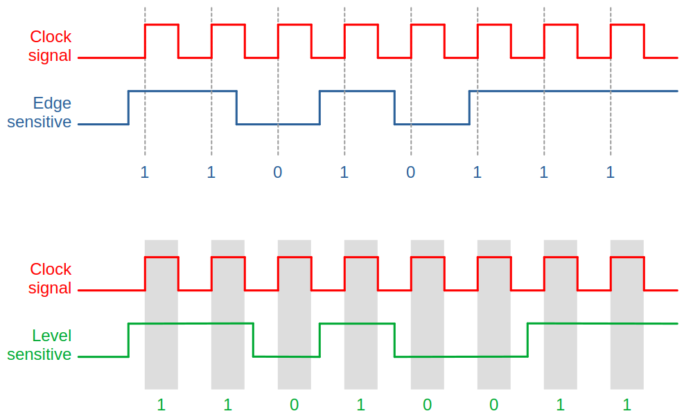
Edge-sensitive (rising edge) and level-sensitive (high level) signal illustration.
💡 If a data signal is edge-sensitive, it must remain stable for a short period before and after the specified clock edge; otherwise, a setup/hold time violation may occur, easily driving the system into a metastable state and affecting functional correctness. This is a hardware limitation that cannot be eliminated and is a challenge in high-frequency digital IC design.
SPI: A Complete and Flexible Communication Protocol
Hardware Configuration
The SPI protocol supports communication between one master and multiple slaves and requires four types of connections.
| Wire Name | Function | Description |
|---|---|---|
SCK |
Clock wire | Generated by the master; polarity and phase selectable |
CS |
Chip Select wire | Determines which slave the master talks to; one per slave, active low |
MOSI |
Master Out Slave In | Data wire; shared by all slaves |
MISO |
Master In Slave Out | Data wire; shared by all slaves |
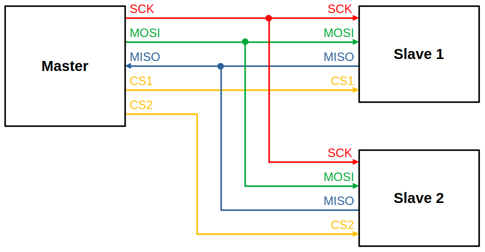
SPI protocol hardware configuration.
The SPI design allows data to be transmitted at extremely high speeds; for example, the STM32G473RCT6 supports a rate of up to 8.0 MBit/s (8 million bits per second). Moreover, because the input and output wires are separate, SPI can achieve full-duplex communication—data sent from the master to the slave and from the slave to the master can be transmitted simultaneously.
Data Transmission
Start and Stop
The SPI chip select wire CS is active low. Therefore, data transmission begins when CS is set low and ends when CS is set high.
Transmission Process
SPI data signals are edge-sensitive. The clock signal is carried on the SCK wire, and we can adjust the clock polarity (CPOL) and clock phase (CPHA) to meet the requirements of different peripherals.
- Clock Polarity (CPOL): The idle state level of the clock. It can be 0 or 1:
- 0 means the clock idles low,
- 1 means the clock idles high.
- Clock Phase (CPHA): Which edge of the clock signal to use for sampling, counted from the start of the clock signal. It can be 0 or 1:
- 0 means use the first edge after the clock signal starts,
- 1 means use the second edge after the clock signal starts.
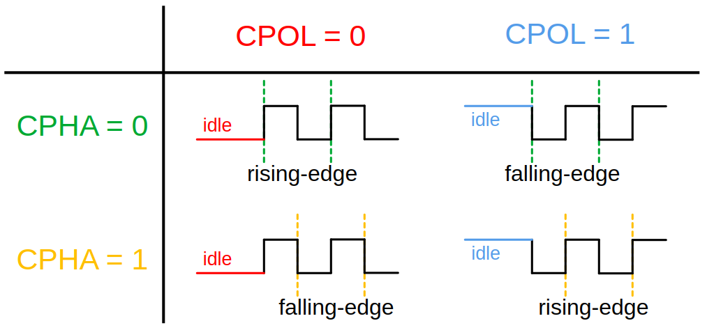
SPI clock polarity and clock phase illustration.
On both the MOSI and MISO data wires, data is sent most significant bit (MSB) first, meaning the higher bits are transmitted before the lower bits. The figure below shows an example of an SPI transmission.
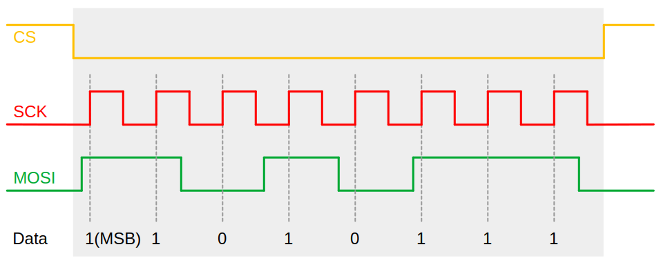
SPI transmission example: master sends data to slave, CPOL = 0, CPHA = 0.
Implementation
SPI can be implemented on an MCU in two ways: software SPI and hardware SPI.
- Software SPI uses general-purpose input/output (GPIO) pins to control the four SPI wires, with the code toggling the GPIOs to transmit data.
- Hardware SPI leverages the MCU’s built-in SPI module. At the code level, you only need to call the corresponding library functions. For instance, on STM32G4 series MCUs, after configuring the relevant pins, you can directly call
HAL_SPI_TransmitandHAL_SPI_Receiveto send and receive data using the on-chip SPI peripheral.
Software SPI typically achieves a lower transfer rate than hardware SPI.
💡 From a broader perspective, a software implementation is generally less efficient than a hardware implementation for the same problem. Software is indirect: all code is ultimately translated into machine instructions and executed on a general-purpose processor, which is not optimized for any specific task. Hardware is direct: the requirement is realized directly in digital logic, creating a dedicated digital circuit designed to solve that particular problem, which can therefore be optimized to the extreme.
A real-world example can be seen in quantitative trading, where calculation speed is critical—a sell order delayed by just a few milliseconds can cause losses of thousands or even tens of thousands of dollars. Beyond squeezing every bit of performance out of software, practitioners have even begun using FPGAs (Field-Programmable Gate Arrays) for relevant computations because they execute faster. An FPGA is a more direct hardware implementation; its internal structure consists of basic logic elements that can be connected through programming to form a digital circuit for a specific function.
Below is an example of software SPI, based on STM32G4 series MCUs.
// CPOL = 0, CPHA = 0
void spi_transmit(const GPIO_TypeDef* CS_port, const uint16_t CS_pin, uint8_t data) {
  HAL_GPIO_WritePin(SCK_port, SCK_pin, GPIO_PIN_RESET); // SCK low, idle
  HAL_GPIO_WritePin(CS_port, CS_pin, GPIO_PIN_RESET);   // CS low, start transmission

  for (int i = 7; i >= 0; --i) { // MSB first
    HAL_GPIO_WritePin(MOSI_port, MOSI_pin, (data & (1 << i)) ? GPIO_PIN_SET : GPIO_PIN_RESET);
    HAL_GPIO_WritePin(SCK_port, SCK_pin, GPIO_PIN_SET);   // SCK high, rising edge
    HAL_GPIO_WritePin(SCK_port, SCK_pin, GPIO_PIN_RESET); // SCK back to low
  }

  HAL_GPIO_WritePin(CS_port, CS_pin, GPIO_PIN_SET);   // CS high, end transmission
  HAL_GPIO_WritePin(SCK_port, SCK_pin, GPIO_PIN_RESET); // SCK low, back to idle
}
I2C: Clever Scheduling of a Single Data Wire
We can see that SPI has one drawback: the number of wires is still relatively high, especially the chip select wire, which requires one per slave. Is there a way to reduce the number of wires?
Thankfully, there is. Take a look at I2C.
Hardware Configuration
The I2C protocol supports communication between multiple masters and multiple slaves. It requires only two wires.
| Wire Name | Function | Description |
|---|---|---|
SCL |
Clock wire | Generated by the master; slaves can stretch the low period according to their processing needs |
SDA |
Data wire | Used for bidirectional data transfer between master and slave |
Since there is no chip select wire, I2C requires each slave in the system to have a unique address so the master can distinguish them.
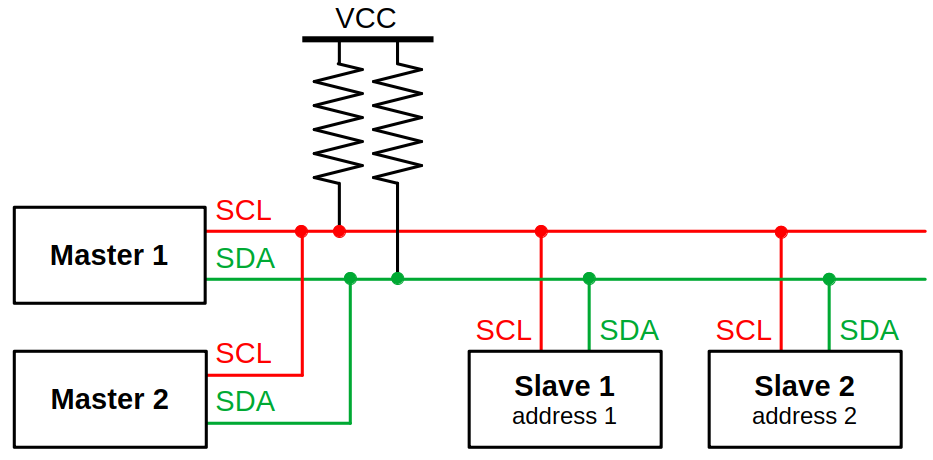
I2C protocol hardware wiring.
Notice that both the SCL clock wire and SDA data wire in I2C are connected to a pull-up resistor. Inside each device, both wires are connected to ground through an NMOS transistor. This relates to the way I2C generates its logic levels:
- When a device wants to output a low level, it turns on its NMOS transistor, pulling the wire to ground.
- When a device wants to output a high level, it turns off its NMOS transistor, releasing the wire, and the pull-up resistor pulls it high.
Therefore, when idle, both wires are at a high level.
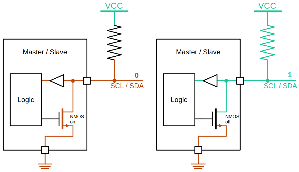
I2C level generation mechanism.
💡 An NMOS transistor is a type of MOSFET (Metal-Oxide-Semiconductor Field-Effect Transistor). It has three terminals: the top-right and bottom-right ports in the figure are the drain and source, and the left port is the gate. In this circuit, the NMOS can be thought of as a switch controlled by the gate voltage: when the gate is low, the drain and source are not conducting (switch open); when the gate is high, they conduct (switch closed).
This connection also creates a wired-AND effect: when multiple devices try to output on the same wire,
- only if all of them want to output a high level will the wire be high;
- conversely, if any device wants to output a low level, the wire becomes low.
I2C exploits this effect to avoid short circuits (VCC directly to ground) and to implement many clever mechanisms, which we will discuss shortly.
However, because the I2C high level is not hard-wired to VCC but is achieved through a pull-up resistor, the power supply must charge the entire wire’s parasitic capacitance through that resistor. The pull-up resistor’s value is generally not very small, so the time constant of this RC circuit is relatively large, making the low-to-high transition fairly slow. This limits the I2C transfer rate, preventing it from reaching SPI levels (e.g., the STM32G473RCT6’s I2C maximum speed is only 400 kBit/s, i.e., 400,000 bits per second).
Furthermore, because there is only one data wire, although a master can send data to a slave and a slave can send data to the master, both cannot happen at the same time. Therefore, I2C can only support half-duplex communication.
Data Transmission
Start and Stop
The I2C start and stop conditions are special:
- START condition: while
SCLis high,SDAtransitions from high to low. - STOP condition: while
SCLis high,SDAtransitions from low to high.
Additionally, there is a repeated START condition, used when the master wants to initiate a new communication without releasing the bus by sending a STOP condition first.
Transmission Process
I2C data signals are level-sensitive. Except during the start and stop conditions, all data on the SDA wire is read while SCL is high. Therefore, during each SCL high period, the level on SDA must remain stable; otherwise it may be interpreted as a start or stop condition, causing errors.
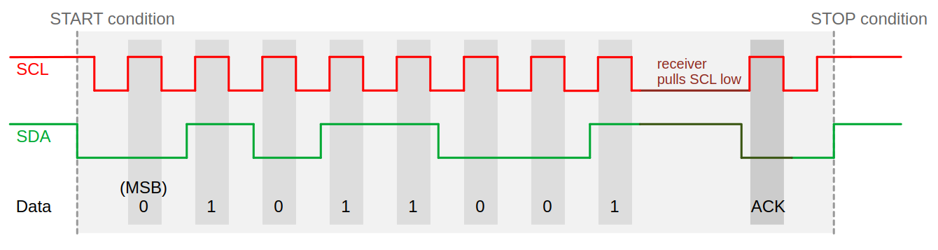
On the SDA data wire, data is sent MSB first and generally in bytes. I2C also introduces an acknowledge (ACK) and not-acknowledge (NACK) mechanism to let the sender know the reception status: after each byte is transmitted, the sender temporarily releases the SDA wire for one clock cycle, and the receiver controls SDA during that cycle:
- A high level indicates NACK: the receiver cannot or does not want to receive more data.
- A low level indicates ACK: the receiver has fully received and processed the data, telling the sender it can proceed with the next operation.
Note that the sender is not necessarily the master, nor is the receiver necessarily the slave. A slave can also send data to the master.
💡 The high/low assignment for ACK and NACK is deliberate: under normal operation, the receiver must actively drive the
SDAwire. If the receiver itself is faulty and completely unresponsive, it will not driveSDA, leaving it at its idle high level: which corresponds to NACK. Upon seeing this, the sender knows that its data was not received.
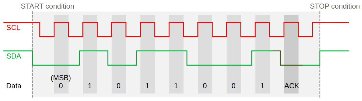
I2C byte transmission process (receiver sends ACK at the end).
I2C data transfers often follow a fixed format. Different slaves may have different requirements, but most include a slave address, an internal register address within the slave, and the actual data to be transferred. The image below is taken from the IS31FL3731 datasheet; it is an LED matrix driver that communicates with an MCU using I2C.
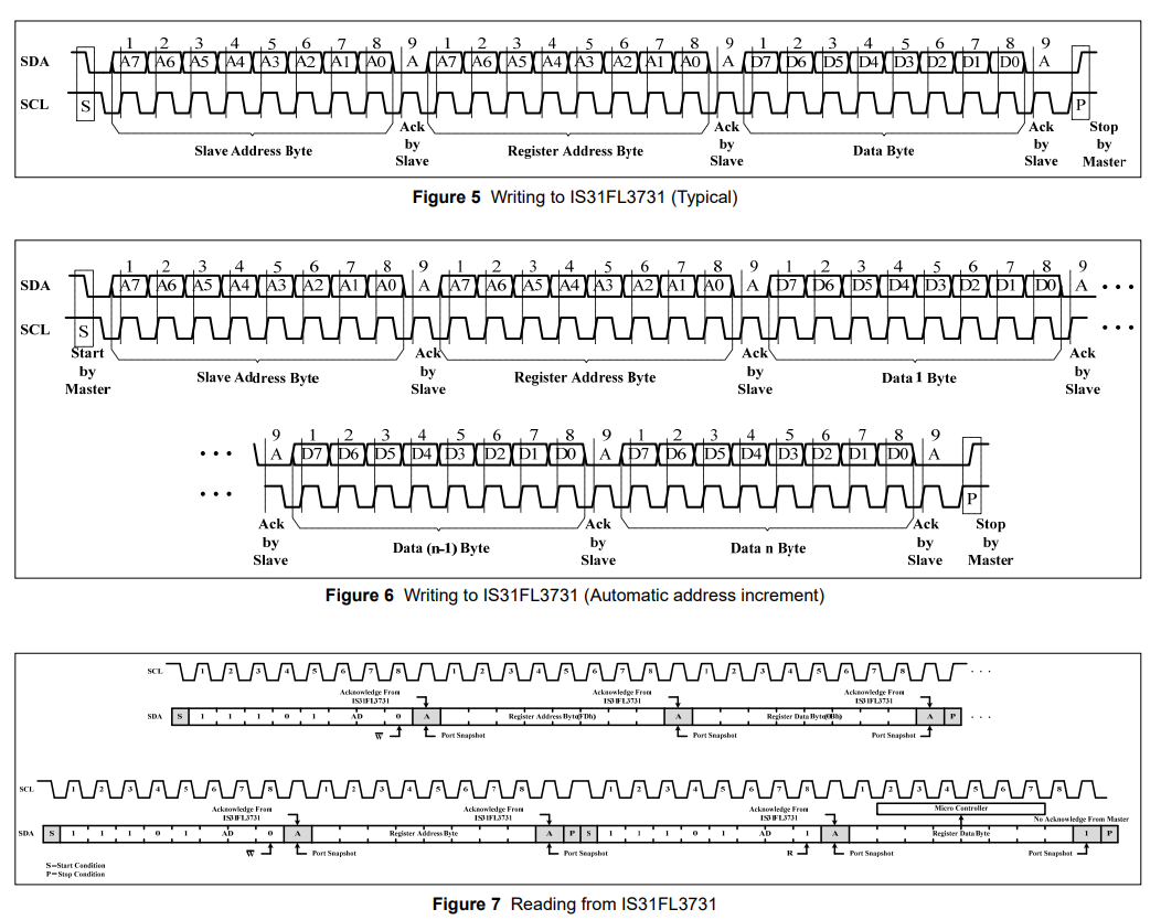
Data transmission format specified by the IS31FL3731. Image from the IS31FL3731 datasheet.
Special Mechanisms
When a multi-master system adopts the I2C protocol, how to orderly and efficiently schedule control of the bus becomes an issue. This is where the “wired-AND” property of I2C shows its power.
Clock Synchronization
Even if multiple masters configure their clock signals to the same frequency, the phase and duty cycle can hardly be perfectly aligned. How can a stable clock be established to ensure that SDA is constant when the clock is high?
We realize that when all the clock signals generated by the individual masters are high, the data they want to output on SDA is meant to be stable, so the level on SDA will definitely be stable. Therefore, the stable clock signal can be obtained by ANDing all the individual clock signals. This requires no extra hardware, because SCL naturally possesses the wired-AND property! This is clock synchronization.
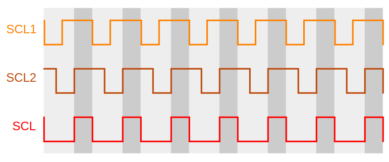
I2C clock synchronization mechanism.
Arbitration
The clocks are synchronized, but multiple masters may still attempt to start transmitting at the same moment, resulting in contention for the bus. I2C resolves this through arbitration.
The rule of arbitration is simple: we cannot prevent masters from starting at the same time, so we simply let them proceed by send their respective data while monitoring the SDA wire. Whichever master first sends a high level on SDA but observes a low level loses arbitration and withdraws. The master that loses arbitration must release SDA and may only try to transmit again after observing a STOP condition. This arbitration mechanism is decentralized—no unified higher-level unit commands it; it relies entirely on the “self-awareness” of each master.
Thanks to the wired-AND property of SDA, when a master loses arbitration and withdraws, it has no impact on the master still transmitting, because the withdrawing master was attempting to send a high level. Before losing, they must have been sending identical data. Therefore, the arbitration process is entirely transparent to all slaves; they cannot detect it.
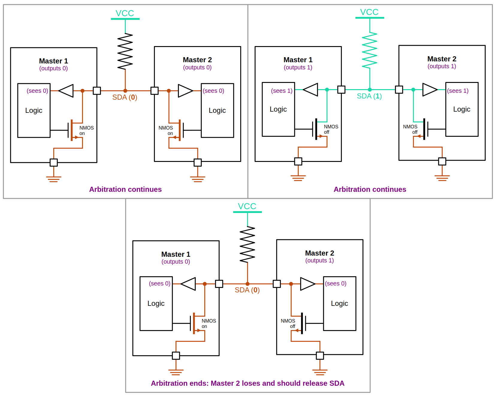
I2C arbitration mechanism.
Clock Stretching
Sometimes a slave needs some time to process data sent by the master. Since the slave does not control the clock, if new data from the master arrives before processing is complete, or if the slave is too busy to pull SDA low in time to acknowledge, the transmission can easily become chaotic and inefficient.
But the slave is not powerless. It can actively pull the SCL wire low to extend the low period of a clock cycle, thereby gaining enough time to finish processing. Because of the wired-AND property of SCL, as long as the slave holds it low, even if the master tries to drive it high, it will remain low. The master, upon observing this, must correspondingly extend the low period of its own generated clock signal until the slave finishes processing and releases SCL. This is clock stretching.
I2C clock stretching mechanism.
Implementation
I2C can also be implemented in both hardware and software on an MCU. However, because the I2C protocol is rather complex, a software implementation would be cumbersome and inefficient; therefore, in the vast majority of scenarios, hardware I2C is used. On STM32G4 series MCUs, after configuring the pins for the I2C module, you can directly call HAL_I2C_Master_Transmit and HAL_I2C_Master_Receive to transmit and receive data via the hardware I2C peripheral.
UART: Removing Clock Wire to Achieve Async Full-Duplex
Although I2C uses only two wires, it has only one data wire SDA and can only achieve half-duplex—like a single-track railway: when two trains traveling in opposite directions meet, one must stop and wait for the other to pass completely. Is there a way to retain the low wire count of I2C while transforming it into a “double-track railway” to achieve full-duplex?
Naturally, we turn our attention to I2C’s other wire, SCL. Its existence makes I2C synchronous. If we replace it with another data wire, we can regain full-duplex, but the transmission becomes asynchronous. This is UART.
Hardware Configuration
The UART protocol supports communication between only two devices and has no strict master/slave distinction, because both devices are constructed identically. Each device has two ports:
RXfor receiving data,TXfor transmitting data.
Each device’s RX is connected to the other device’s TX. This achieves full-duplex communication, allowing both devices to exchange data simultaneously.
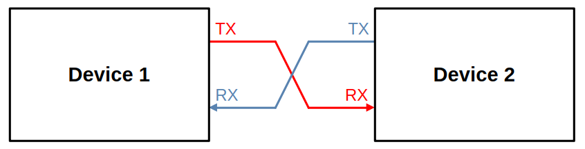
UART protocol hardware wiring.
💡 Generally, UART is used for communication between a PC and an MCU. In this context, the PC is often referred to as the host computer.
Data Transmission
Start and Stop
RX/TX are idle high. A transmission starts when the wire transitions from high to low; after the data is transmitted, the wire transitions back from low to high, stopping the transmission. The start and stop conditions each occupy the time of one data bit and are called the start bit (START bit) and stop bit (STOP bit).
Transmission Process
Since there is no common clock to orchestrate them, the two devices must agree on many things in advance, including the baud rate. Baud rate refers to the number of symbols transmitted per second, measured in the unit of baud. In the UART context, baud rate equals the number of bits transmitted per second, because each bit is carried by one symbol in the signal. Common UART baud rates include 9600, 19200, and 115200.
Even when the baud rate is set identically, the receiver only sees a bare data signal. If it samples this signal only once per bit period, severe errors can easily occur because there is no reference point. UART solves this with start-bit synchronization and oversampling: the receiver begins receiving data only after observing a start bit, and it samples the data signal at a multiple of the agreed baud rate. This multiple is typically a power of two, commonly 8, 16, or 32.
Taking 16× oversampling as an example, there are 16 sampling periods per data bit. The receiver’s sampling flow is as follows:
- Observe
RXtransitioning from high to low; begin sampling. - After 8 sampling periods, check whether
RXis still low. If so, treat this as the center of the start bit; if not, the previously observed transition was a noise glitch, and sampling stops. - Sample
RXevery 16 sampling periods, using each as the center of a new data bit. - Stop sampling after all data bits have been received.
Additionally, the two devices must agree on how many data bits are sent between the start and stop bits, and must stay consistent throughout the communication. We can also choose to append a parity bit after the data, indicating whether the transmitted data should contain an even or odd number of high bits, allowing the receiver to check for errors.
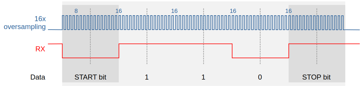
UART data transmission: 16× oversampling, 3 data bits, no parity bit.
Of course, just as two synchronized clocks will drift over time, the two devices’ individual baud rates may also have slight differences, causing error accumulation. In theory, however, the impact is small because:
- Before each data transmission, start-bit synchronization resets the timing, limiting error accumulation to within a single frame.
- By oversampling and choosing an appropriate sampling instant, we ensure that each sample is taken near the nominal center of the data bit; even a slight drift is unlikely to read the wrong level.
In practice, the UART protocol can tolerate a baud rate error of around 4% between the two devices.
Implementation
The UART protocol is generally implemented via dedicated hardware, requiring only calls to the corresponding low-level functions in code.
Beyond the provided low-level functions, many open-source UART libraries are available that greatly simplify debugging and development. For example, SerialAccessor is a serial debugging framework that enables a host computer to directly access MCU registers over UART. If time permits, I will also analyze the operating mechanism of this framework in detail, including topics such as DMA buffers.
Summary
We have covered the fundamental principles of the SPI, I2C, and UART serial communication protocols in detail. In practice, you can choose among them flexibly based on their characteristics and your actual requirements.
| Protocol | Timing | Duplex | Device Count | Wire Count | Slave Select | Transfer Rate |
|---|---|---|---|---|---|---|
| SPI | Sync | Full | single-master, multi-slave | At least 3 | Chip select CS |
Very high |
| I2C | Sync | Half | Multi-master, multi-slave | 2 | Slave address | Relatively low |
| UART | Async | Full | One-to-one | 2 | - | Relatively low |
References
- Understanding the SPI Bus (SBOA621) - Texas Instruments
- Understanding the I2C Bus (SLVA704) - Texas Instruments
- Basics of I2C: Advanced Topics (TIPL6104) - Texas Instruments
- UART Protocol Overview - Texas Instruments
- IS31FL3731: Audio Modulated Matrix LED Driver - Lumissil Microsystems
- Description of STM32G4 HAL and low-layer drivers (UM2570) - ST Microelectronics